

Systems and methods for non-contact measuring sputtering target thickness ultrasonics
a non-contact, target thickness technology, applied in the direction of instruments, specific gravity measurement, wave/particle radiation for converting sensor output, etc., can solve the problem of not always being able to flatten the bond interface, the bond interface deflects from an originally predefined shape, and the pre-designed shape of the bond interface is difficult to maintain. the effect of improving the probability of finding
- Summary
- Abstract
- Description
- Claims
- Application Information
AI Technical Summary
Benefits of technology
Problems solved by technology
Method used
Image

Examples
Embodiment Construction
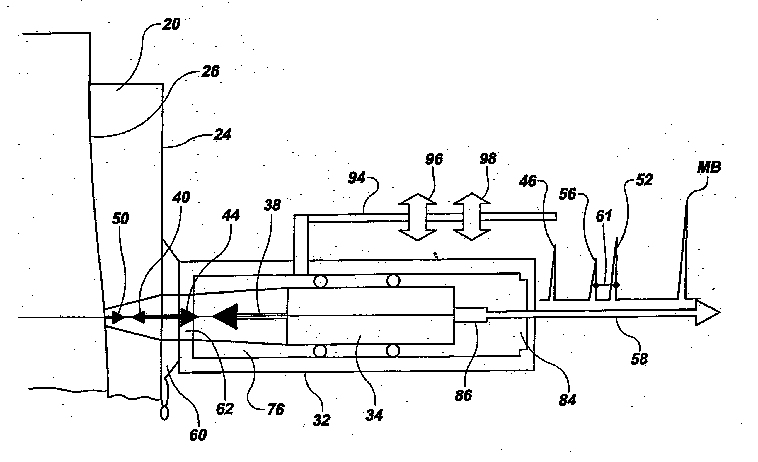
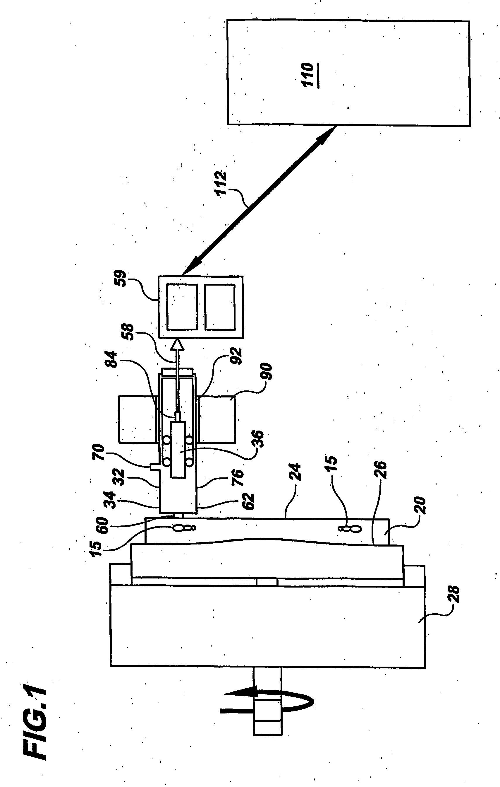
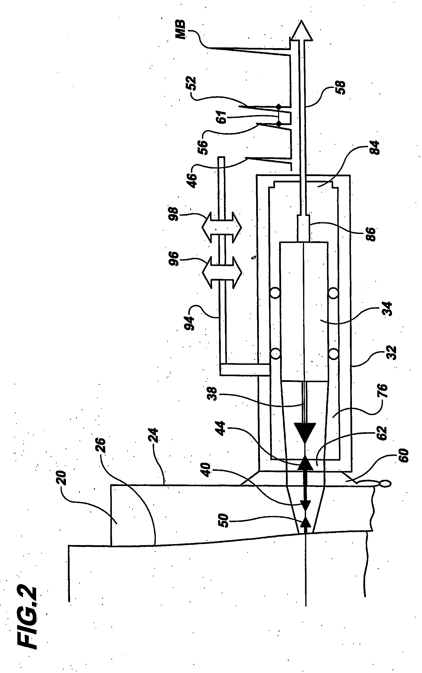
[0028] Turning to FIGS. 1 and 2, there may be seen schematic diagrams illustrating the method of instant invention. In accordance with this method, a test target specimen 20 of a bonded target assembly having a planar front surface 24 and non-flat but smooth bonded surface 26 is mounted into chuck 28 of a machining tool. The machining tool rotates the specimen 20 axially symmetrically. Ultrasonic transducer 36 with a flat surface is mounted inside a bubbler 32. The transducer 36 is positioned axially symmetrical with a nozzle 34 at some distance from nozzle opening. The bubbler 32 is placed near the front surface 24 of specimen 20 preferably adjacent the sputter track 15 which is well known in the art as a particular section or region of the target that is most heavily consumed during the sputtering process. The transducer 36 irradiates the front surface 24 of the test specimen 20 with a single, short-duration, megahertz frequency range ultrasonic pulse 38 propagating through column...
PUM
| Property | Measurement | Unit |
|---|---|---|
| peak frequency | aaaaa | aaaaa |
| ultrasonic thickness | aaaaa | aaaaa |
| sonic energy | aaaaa | aaaaa |
Abstract
Description
Claims
Application Information