

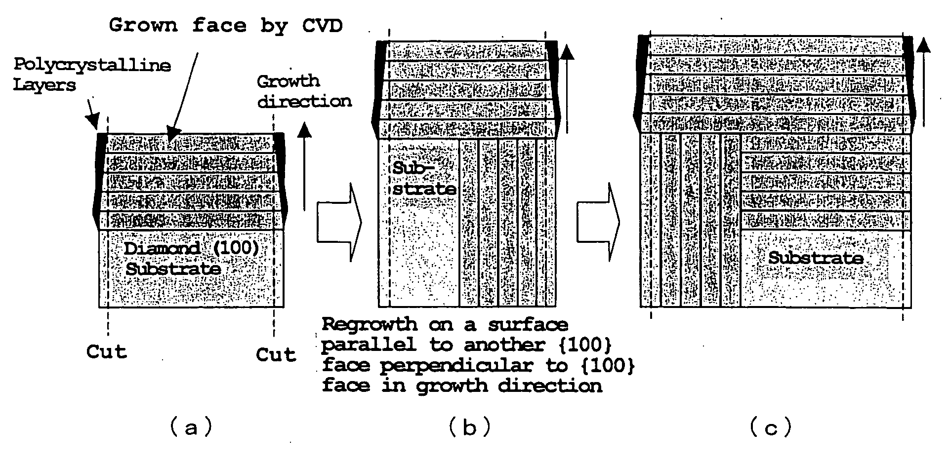
Method of producing single crystal
a single crystal, crystal technology, applied in the direction of crystal growth process, polycrystalline material growth, pressurized chemical process, etc., can solve the problems of difficult to produce large single crystal diamonds, extremely low growth rate, and long processing time, so as to achieve the effect of large single crystal diamond and low cos
- Summary
- Abstract
- Description
- Claims
- Application Information
AI Technical Summary
Benefits of technology
Problems solved by technology
Method used
Image

Examples
example 1
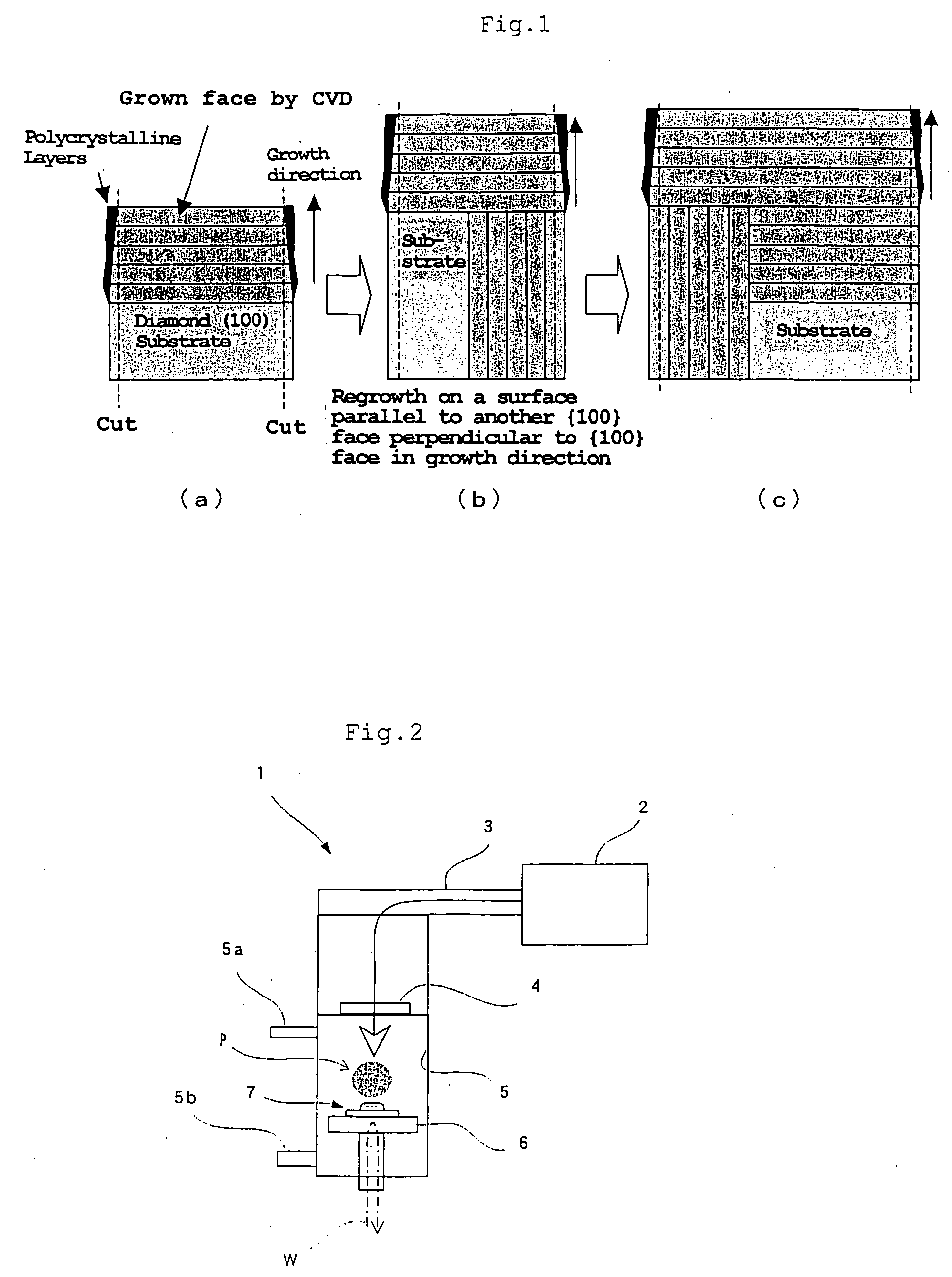
[0120] A single-crystal diamond obtained by a high-pressure high-temperature synthetic method was cut parallel to a {100} face and polished to obtain a 3×3×0.5 mm3 tabular crystal as a diamond seed crystal, which was then placed on a substrate (diamond seed crystal) holder in a microwave plasma CVD apparatus (FIG. 2) provided with a cavity resonator-type reaction chamber.
[0121] The reaction chamber was evacuated, H2 gas was introduced, the pressure in the reaction chamber was set to 10 Torr (1333 Pa), and microwave power of 500 W at a frequency of 2.45 GHz were applied to generate plasma. Subsequently, the reactor pressure, H2 gas flow rate and microwave power were gradually increased to ensure a pressure of 160 Torr (21.3 kPa) and a H2 gas flow rate of 500 cc (standard conditions) / min. Then, the substrate temperature was set at 1130° C. while the microwave power was kept between 1000 and 3000 W, and N2 gas and CH4 gas were introduced at flow rate of 0.6 cc (standard conditions) / mi...
example 2
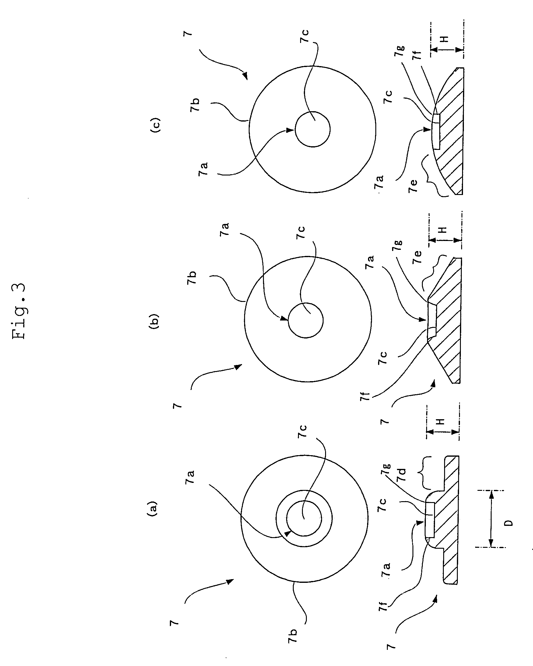
[0127] In the microwave plasma CVD system (FIG. 2) used in Example 1, a diamond crystal was grown using as a substrate (single-crystal diamond) holder a molybdenum holder. The holder had a structure in which a member comprising a holding portion was dissociated from a member comprising an outer peripheral portion, as shown in FIG. 5. A single-crystal diamond obtained by a high-pressure high-temperature synthetic method was cut parallel to a {100} face and polished to obtain an octagonal tabular crystal of about 0.5 mm thickness for use as a seed crystal.
[0128] The growth steps were the same as in Example 1. The growth conditions were a pressure of 180 Torr (24 kPa), H2 gas flow rate of 500 cc (standard conditions) / min., N2 gas flow rate of 0.6 cc (standard conditions) / min., and CH4 gas flow rate of 60 cc (standard conditions) / min. Further, microwave power was adjusted between 1540 and 2550 W to ensure a growth temperature of 1130° C.
[0129] For the first crystal growth, used was th...
example 3
[0133] Using the microwave plasma CVD system (FIG. 2) as used in Example 1, a diamond crystal was grown using a molybdenum substrate holder having a structure as shown in FIG. 6. The same single-crystal diamond as used in Example 1 was used as a seed crystal.
[0134] Crystal growth was performed in the same manner as in Example 1, with the growth conditions under a pressure of 180 Torr (24 kPa), H2 gas flow rate of 500 cc (standard conditions) / min., N2 gas flow rate of 0.6 cc (standard conditions) / min., and CH4 gas flow rate of 60 cc (standard conditions) / min. Further, the microwave power was adjusted between 2390 and 2830 W to ensure a growth temperature of 1160° C.
[0135] For the first crystal growth, the holder used had a holding portion having a cylindrical recessed shape with a diameter of 5 mm and a depth d2 of 1 mm. The single-crystal diamond was placed in the center of this recessed portion so that the surface of the single-crystal diamond had a distance (d) of 0.5 mm to the ...
PUM
| Property | Measurement | Unit |
|---|---|---|
| frequency | aaaaa | aaaaa |
| frequency | aaaaa | aaaaa |
| pressure | aaaaa | aaaaa |
Abstract
Description
Claims
Application Information