Semiconductor device and manufacturing method thereof

a semiconductor and manufacturing method technology, applied in semiconductor devices, solid-state devices, decorative arts, etc., can solve the problems of inability to achieve cost reduction in a step using a small single crystalline silicon substrate or quartz substrate, difficult to prepare a large apparatus in accordance with a large glass substrate or uniform polishing of a large glass substrate, etc., to achieve high flatness, high toughness, and high yield

Inactive Publication Date: 2006-11-30
SEMICON ENERGY LAB CO LTD
View PDF8 Cites 33 Cited by
  • Summary
  • Abstract
  • Description
  • Claims
  • Application Information

AI Technical Summary

Benefits of technology

[0035] Grinding and polishing are used for making a non-single crystalline thin film transistor element manufactured over such a semiconductor substrate into a thin element such as an IC chip. An edge defect or a crack is easily generated in a square glass substrate; however, the problems are reduced in a round polycrystalline substrate or a single crystalline substrate, and yield is increased.
[0036] Moreover, a silicon material has high toughness than a glass material, and thus, the silicon material is suitable for being polished thinner. In particular, a polycrystalline substrate has intensity without a breaking in a manner cutting the substrate vertically, which is seen in a single crystalline substrate. In addition, the polished silicon material with a high degree of flatness has a variation within submicron in its plain, and can...

Problems solved by technology

However, there are various restrictions on the shape, step, or the like in the case of manufacturing a thin element using a glass substrate as a base material.
However, it is difficult to prepare a large apparatus in accordance with a large glass substrate or to polish a large substrate uniformly.
Thus, there is a problem such that cost reduction in a step using a small single crystalline silicon substrate or a quartz substrate cannot be achieved.
Thus, cost tends to increase.
In addition, a substrate having corners is unsuitable for a grinding and polishing apparatus having a rotational friction structure, and there is a problem such that a corner defect and crack is easily produced.
Therefore, a round substrate having an excellent symmetric as a single crystalline substrate ...

Method used


Image

  • Semiconductor device and manufacturing method thereof
  • Semiconductor device and manufacturing method thereof
  • Semiconductor device and manufacturing method thereof

Examples


embodiment mode 1

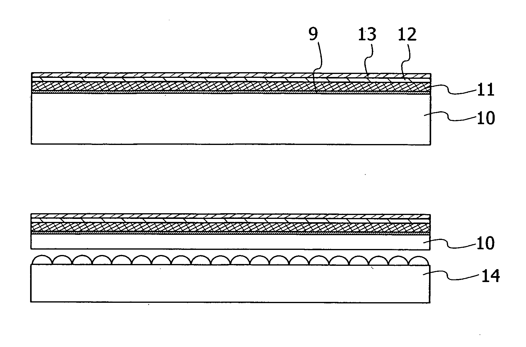
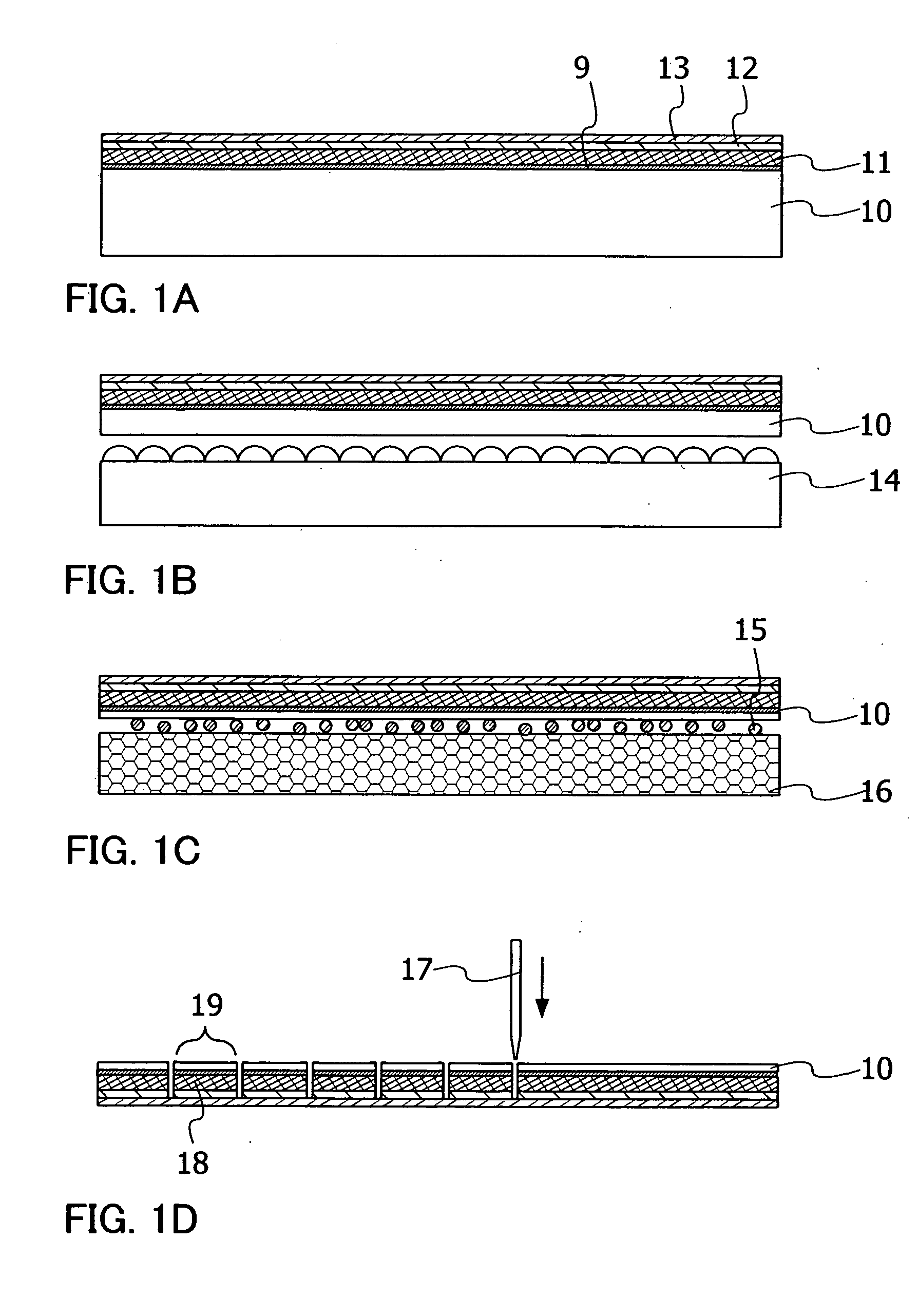
[0059] A thin film integrated circuit device and a manufacturing method thereof using the present invention are described with reference to accompanying FIGS. 1A to 3C. First of all, a substrate 10 made with a silicon wafer is prepared as a support substrate, and a first insulating film 9 is formed by heat treatment or a film forming method (refer to FIG. 1A), for example, a high-density plasma treatment apparatus, a sputtering apparatus, a plasma CVD apparatus, a vacuum pressure CVD apparatus, or the like. Note that it is preferable that the surface of a silicon substrate be directly processed with a high-density plasma treatment apparatus. The first insulating film 9 is formed with an oxide film, a nitride film, or an oxynitride film of silicon. Note that a polycrystalline silicon substrate whose surface is mirror-polished or a single crystalline substrate is preferably used for the silicon wafer serving as the support substrate. Herein, in the case of using the single crystalline...

embodiment mode 2

[0082] Embodiment Mode 2 of the present invention will be described referring to FIGS. 4A to 6B.

[0083] First, an insulating film 32 is formed over one surface of a substrate 30, and a layer 31 having a plurality of thin film integrated circuits is formed over the insulating film 32 (refer to FIG. 4A). Note that the substrate 30 corresponds to a silicon wafer, for example a polycrystalline silicon substrate or a single crystalline substrate. The layer 31 having a plurality of thin film integrated circuits includes at least a plurality of insulating films, a semiconductor layer and a conductive layer making up a plurality of elements.

[0084] Next, a film 33 is provided so as to cover the layer 31 having a plurality of thin film integrated circuits. The film 33 is formed with a vinyl chloride resin, a silicone resin, a polyolefin resin, or the like, and a film having a stretching property is used. Thus, the film 33 is called as an expanded film in some cases. In addition, the film 33 ...

embodiment mode 3

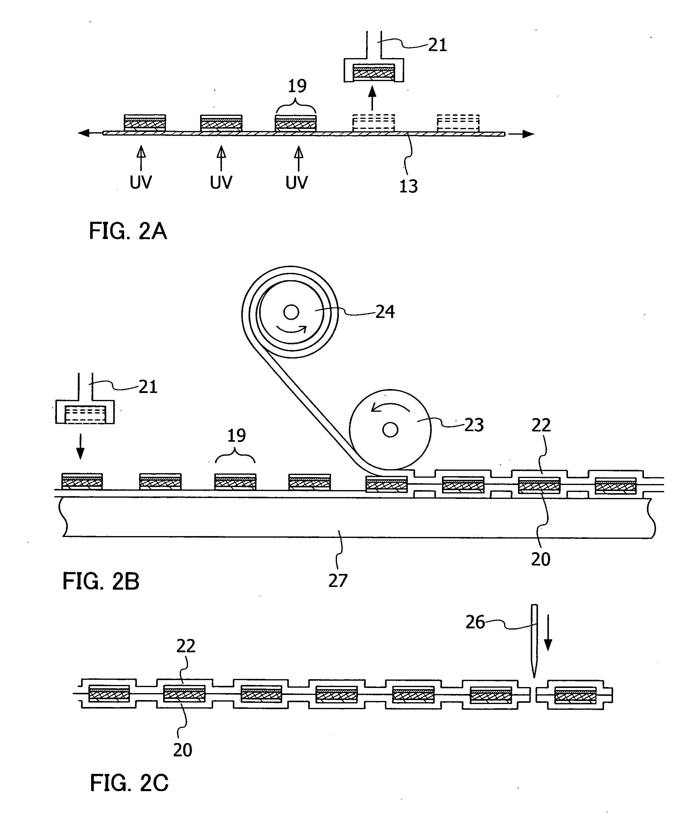
[0097] Embodiment Mode 3 of the present invention is described referring to FIGS. 7A to 9. In the present embodiment mode, operation using a frame (carrier jig) in the step of Embodiment Mode 1 is described.

[0098] First of all, the insulating film 9 is formed over the substrate 10, and the layer 11 having a plurality of thin film integrated circuits is formed over the insulating film 9 as described above. Subsequently, the first film or the resin layer 12 is pasted so as to cover the layer 11 having a plurality of thin film integrated circuits. Then, the second film 13 is pasted so as to cover the first film or the resin layer 12. This step is conducted by setting a stack 52 of the first film or the resin layer 12, the layer 11 having a plurality of thin film integrated circuits, and the substrate 10 over the second film 13 attached to a frame 51 (refer to a cross-sectional view of FIG. 7A, and, a perspective view of FIG. 7B).

[0099] A porous chuck 53 is set so as to touch one surf...


PUM

PropertyMeasurementUnit
Thicknessaaaaaaaaaa
Thicknessaaaaaaaaaa
Thicknessaaaaaaaaaa

Abstract

To provide a thin film integrated circuit at low cost and with thin thickness, which is applicable to mass production unlike the conventional glass substrate or the single crystalline silicon substrate, and a structure and a process of a thin film integrated circuit device or an IC chip having the thin film integrated circuit. A manufacturing method of a semiconductor device includes the steps of forming a first insulating film over one surface of a silicon substrate, forming a layer having at least two thin film integrated circuits over the first insulating film, forming a resin layer so as to cover the layer having the thin film integrated circuit, forming a film so as to cover the resin layer, grinding a backside of one surface of the silicon substrate which is formed with the layer having the thin film integrated circuit, and polishing the ground surface of the silicon substrate.

Description

BACKGROUND OF THE INVENTION [0001] 1. Field of the Invention [0002] The present invention relates to a manufacturing method of a semiconductor device including a flexible thin film integrated circuit having a memory, a microprocessor (central processing unit, a CPU), or the like with a thin thickness like paper. The present invention further relates to a manufacturing method of a non-contact type thin film integrated circuit device including the thin film integrated circuit and an antenna, which is used for a card, a tag, a label, or the like to distinguish human, animals and plants, products, paper money, or the like mainly. [0003] 2. Description of the Related Art [0004] In recent years, development of a semiconductor device which can transmit / receive data is actively advanced, and such a semiconductor device is called as an IC chip, an RF tag, a wireless tag, an electronic tag, a wireless processor, a wireless memory, or the like. Most semiconductor devices, which have been alrea...

Claims


Application Information

Patent Timeline
IPC IPC(8): H01L29/04H01L21/461C03C15/00H01L31/036
CPCH01L27/1266H01L27/1214
Inventor KUSUMOTO, NAOTOTSURUME, TAKUYA
Owner SEMICON ENERGY LAB CO LTD
Why Eureka
Try Eureka