Vertical FET with nanowire channels and a silicided bottom contact

Active Publication Date: 2006-12-07
GLOBALFOUNDRIES US INC
View PDF4 Cites 110 Cited by
  • Summary
  • Abstract
  • Description
  • Claims
  • Application Information

AI Technical Summary

Benefits of technology

[0009] The present invention provides a vertical FET with nanowire channels. Each vertical FET of the present invention includes a plurality of nanowire channels. The nanowires used as the channels of the inventive vertical FET are formed over a crystalline conductive layer, such as a silicide layer, to reduce the access series resistance to the source. The nanowires are surrounded by a gate material

Problems solved by technology

First, it is difficult to efficiently contact the source (or drain) at the bottom of the pillar.
This difficulty results in a relatively high access series resistance to the source (or drain).
Second, doping cannot be achieved by implantation, but rather by in-situ doping during epitaxy, or diffusion from solid sources.
Fourth, the channel surface is defined by etching of the pillar or by epitaxial growth from a trench; etching typically leaves rough walls with reactive-ion etch (RIE) damage, while constrained epitaxy also exhibits defects.
This is very difficult to do because of the incompatibility with ion-implantat

Method used


Image

  • Vertical FET with nanowire channels and a silicided bottom contact
  • Vertical FET with nanowire channels and a silicided bottom contact
  • Vertical FET with nanowire channels and a silicided bottom contact

Examples


Example

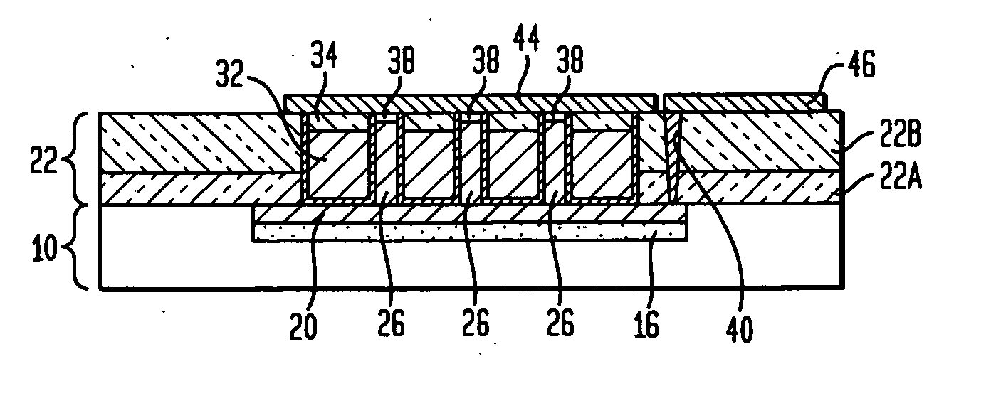
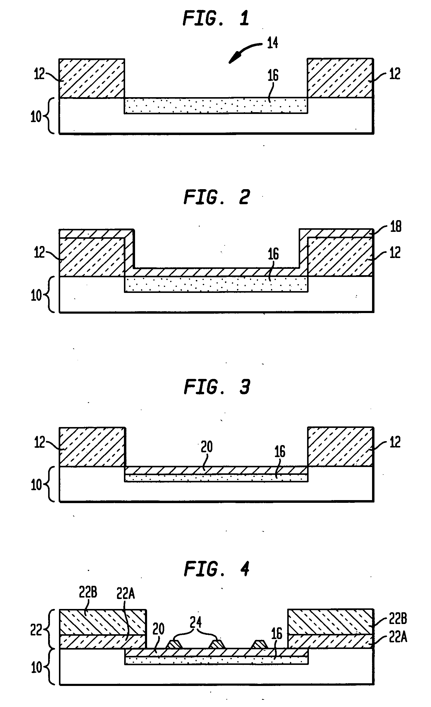
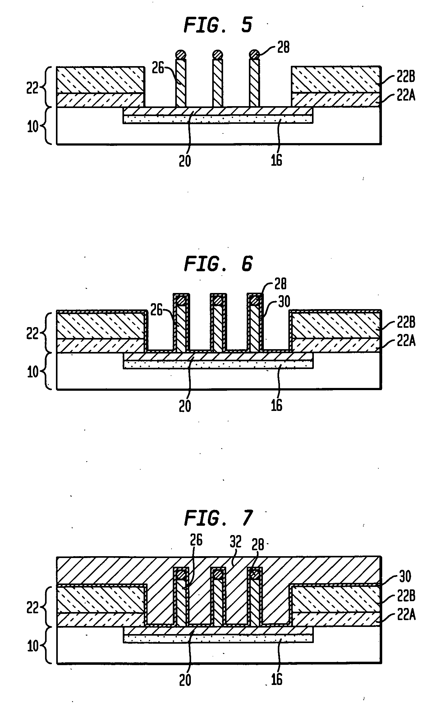
[0021] The present invention, which provides a vertical FET with nanowire channels as well as methods for fabricating the same, will now be described in greater detail by referring to the following discussion. In this discussion, reference will be made to various drawings that illustrate embodiments of the present invention. Since the drawings of the embodiments of the present invention are provided for illustrative purposes, the structures contained therein are not drawn to scale.

[0022] It is again emphasized that the method of the present invention is described using silicon nanowires and silicon processing. The inventive method can also be practiced with other semiconductors such as Ge or III-V semiconductors. When non-Si-containing semiconductors are used, the processing steps of the present invention are basically the same except that a layer of Si can be formed atop the non-semiconductor surface prior to forming the silicide contact layer. Use of Si-containing semiconductor m...


PUM


Abstract

A vertical FET structure with nanowire forming the FET channels is disclosed. The nanowires are formed over a conductive silicide layer. The nanowires are gated by a surrounding gate. Top and bottom insulator plugs function as gate spacers and reduce the gate-source and gate-drain capacitance.

Description

FIELD OF THE INVENTION [0001] The present invention relates to electronic devices based on semiconductor nanowires, and more specifically to a vertical field effect transistor (FET) with nanowire channels and a silicided bottom contact. The present invention also relates to methods of fabricating the vertical FET containing nanowire channels and a silicided bottom contact. BACKGROUND OF THE INVENTION [0002] Conventional vertical FETs are devices in which the source-drain current is flowing in a direction perpendicular to the substrate surface. For example, if the substrate surface is made horizontal, then the vertical FET is typically a vertical pillar with the drain and source being the top and bottom portion of the pillar. One of the main advantages of the vertical FET is that the channel length is not defined by lithography, but rather by methods such as epitaxy or layer deposition which provide good thickness control even at nanometer dimensions. Some examples of vertical FET ar...

Claims


Application Information

Patent Timeline
IPC IPC(8): H01L29/76
CPCB82Y10/00Y10S977/938H01L21/02381H01L21/02433H01L21/02521H01L21/02532H01L21/02603H01L21/0262H01L21/02645H01L21/02653H01L29/045H01L29/0665H01L29/0673H01L29/0676H01L29/66666H01L29/7827H01L29/7828Y10S977/762H01L21/0237
Inventor COHEN, GUY MOSHESOLOMON, PAUL M.
Owner GLOBALFOUNDRIES US INC
Why Eureka
Try Eureka