Process for making an organic light-emitting device

a technology of organic light-emitting devices and electroluminescent devices, which is applied in the direction of discharge tubes/lamp details, luminescent screens of discharge tubes, natural mineral layered products, etc., can solve the problems of organic materials used in the manufacture of oled devices that are often subject to degradation, changes in the structure of molecules, and associated changes in material properties, so as to improve the control and spatial homogeneity of deposition, improve the performance of oled devices, and improve the spatial homo

Inactive Publication Date: 2006-12-07
EASTMAN KODAK CO
View PDF31 Cites 37 Cited by
  • Summary
  • Abstract
  • Description
  • Claims
  • Application Information

AI Technical Summary

Benefits of technology

[0029] The method of OLED device manufacture by the present invention provides a process to continuously deposit multicomponent, organic, EL materials on a substrate, that does not require high temperature nor high vacuum, while improving the control and spatial homogeneity of the deposition. This results in improved OLED device performance while simultaneously achieving a higher degree of spatial uniformity of luminescent dopants. In accordance with various embodiments of the invention, effective organic electroluminescent devices ma

Problems solved by technology

However, despite these advantages, the extent of OLED penetration into the display marketplace has been limited by manufacturing difficulty and high cost.
The organic materials used in the manufacture of OLED devices are often subject to degradation when maintained at or near the desired rate-dependent vaporization temperature for extended periods of time.
Exposure of sensitive organic materials to higher temperatures can cause changes in the structure of the molecules and associated changes in material properties.
In this manner, the material is consumed before it has reached the temperature exposure threshold to cause significant degradation.
The limitations with this practice are that the available vaporization rate is very low due to the limitation on heater temperature, and the operation time of the source is very short due to the small quantity of material present in the source.
The low deposition rate and frequent source recharging place substantial limitations on the throughput of OLED manufacturing facilities.
A secondary consequence of heating the entire organic material charge to roughly the same temperature is that it is impractical to mix additional organic materials, such as dopants, with a host material unless the vaporization behavior and vapor pressure of the dopant is very close to that of the host material.
This is generally not the case and, as a result, prior art devices frequently require the use of separate sources to co-deposit host and dopant materials.
A small change in source temperature may lead to a very large change in vaporization rate.
Despite this, prior-art devices employ source temperature as the only way to control vaporization rate.
These measures have the desired effect on steady-state vaporization rate s

Method used


Image

  • Process for making an organic light-emitting device

Examples


example 1 (

Control)

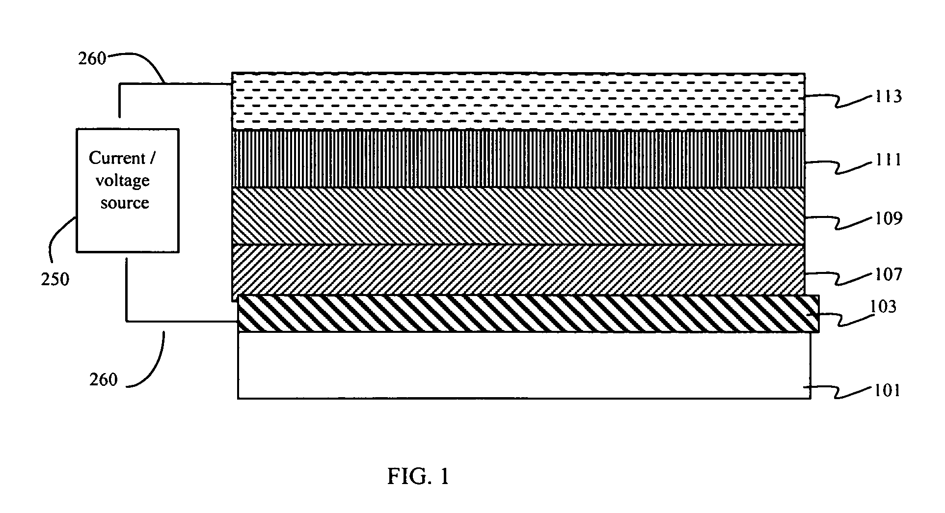
[0121] An OLED device with the structure depicted in FIG. 1 was prepared with the organic EL element layers between the electrodes vacuum deposited by standard techniques. The glass (1143 microns) substrate 101 and Indium Tin Oxide (ITO 100 nm) anode 103 had a replicated pattern geometry divided into four similar quadrants. Subsequently deposited onto this anode structure were: a nominally 50 nm NPB hole-transporting layer 107, a 50 nm light-emitting layer 109 containing TBADN (Tert-Butyl-anthracene di-naphthylene) co-doped with 1 weight % TBP (2,5,8,11 tetra-t-butylperylene) w.r.t. TBADN and 2 weight % NPB (N,N′-di(naphthalene-1-yl)-N,N′-diphenyl-benzidine, a hole-transport material) w.r.t. TBADN, a 37.5 nm ALQ electron- transporting layer 111 and finally a 220 nm thick Mg:Ag cathode 113, and the structure packaged as a functional electroluminescent device.

example 2 (

Invention)

[0122] An OLED device was fabricated similarly as in Example 1, with the exception that the organic material light-emitting layer 109 comprising TBADN and co-dopants TBP and NPB was deposited by a method in accordance with the present invention under atmospheric conditions. More particularly, a SAS type particle generation process of the type disclosed in copending, commonly assigned U.S. Ser. No. 10 / 814,354 (Docket 86430) was employed to generate a desired gaseous flow stream. A nominally 1800 ml stainless steel particle formation vessel was fitted with a 4 cm diameter agitator of the type disclosed in U.S. Pat. No. 6,422,736, comprising a draft tube and bottom and top impellers. CO2 was added to the particle formation vessel while adjusting temperature to 90 C. and pressure to 300 Bar and while stirring at 2775 revolutions per minute. The addition of CO2 at 100 g / min through a feed port that had a 200 μm orifice at its tip, and a 0.1 wt % solution of TBADN co-doped with ...


PUM

PropertyMeasurementUnit
Thicknessaaaaaaaaaa
Areaaaaaaaaaaa
Nanoscale particle sizeaaaaaaaaaa

Abstract

In accordance with one embodiment, the present invention is directed towards a process for forming an organic electroluminescent device comprising depositing on a substrate at least first and second electrode layers and an organic EL element comprising one or more organic material layers between the first and second electrode layers, wherein at least one organic material layer of the EL element is deposited by providing a continuous stream of amorphous solid particles of organic material suspended in at least one carrier gas, the solid particles having a volume-weighted mean particle diameter of less than 500 nm, and depositing particles of the organic material to form a thin uniform layer of the organic material on the substrate surface.

Description

CROSS-REFERENCE TO RELATED APPLICATION [0001] Reference is made to concurrently filed, co-pending application U.S. Ser. No. ______ (Kodak Docket No. 88603) by Rajesh V. Mehta et al entitled “Deposition of Uniform Layer of Desired Material” filed simultaneously herewith, the disclosure of which is incorporated by reference herein.FIELD OF INVENTION [0002] This invention relates to organic electroluminescent (EL) devices. More specifically, this invention relates to a process for deposition of organic material layers in such devices. BACKGROUND OF THE INVENTION [0003] Organic electroluminescent (EL) devices have been known for over two decades, and have many desirable features such as low driving voltage, high luminance, wide-angle viewing and capability for full-color flat emission displays. Tang et al. described a multilayer organic light emitting device (OLED) in their U.S. Pat. Nos. 4,769,292 and 4,885,211. However, despite these advantages, the extent of OLED penetration into the...

Claims


Application Information

Patent Timeline
IPC IPC(8): H01L51/50H01L51/56
CPCH10K71/16H10K71/00
Inventor MEHTA, RAJESHJAGANNATHAN, RAMESHHOUGHTALING, BRADLEYLINK, ROBERTROBINSON, KELLYSPROUT, ROSS
Owner EASTMAN KODAK CO
Why Eureka
Try Eureka