Post passivation structure for a semiconductor device and packaging process for same

a semiconductor device and structure technology, applied in the field of semiconductor devices, can solve the problems of reducing the service life of the device, limiting the ability to meet the increasing demand for finer pitch resolution, and the potential risk of stress-induced failure, so as to reduce the lateral displacement of the rdl, fine pitch contact structure, and relieve stress

Active Publication Date: 2006-12-28
QUALCOMM INC
View PDF8 Cites 82 Cited by
  • Summary
  • Abstract
  • Description
  • Claims
  • Application Information

AI Technical Summary

Benefits of technology

[0027] In accordance with the present invention, the thin support layer serves to provide a thin ramp for step coverage by the RDL, which results in reduced lateral displacements of the RDL even for small ramp slopes, and consequently fine pitch contact structures for a next level packaging structure. Further, the overall thick support structure serves to provide support to the fine pitch conducting posts and relieve stress in the bonded structure above the semiconductor device (e.g., an IC chip). For example, the stress generated by the bonded structure between the semiconductor device and a next level packaging structure (e.g., BGA carrier package substrate) can be accommodated by the thick polymer layer. Such stress can be generated by, for example, the mismatch of thermal expansion between two bonded structures, namely the carrier package substrate and the silicon substrate. Malfunction due to mechanical failure of the IC chips thus can be reduced. Still further, the thick support structure serves to electrically decouple the semiconductor device from the external contact structures and other electrical circuits and structures in the next level packaging structure, as there is reduced capacitance in view of

Problems solved by technology

While WLP is a high throughput and low cost approach to IC chip packaging, it however invites significant challenges in manufacturability and structural reliability.
While the post passivation structures and related processes provide for IC packaging with improved pitch resolution, there is still a limitation to meeting the increasing demand for finer pitch resolution in view of the ever increasing scale of integration in ICs.
There is also potential risk for stress-induced failures, as noted below.
Because the post extends beyond the surface of the polymeric layer, and the top surface of the structure is otherwise not smooth, high-resolution lithography cannot be achieved to form the vias for the conductive posts and to plate the solder bumps.
Consequently, the pitch of the contacts for the IC package would be limited.
Further, as noted, the bottom polymeric layer is separate from the top polymeric layer, therefore the bottom polymeric layer alone does not provide good stress re

Method used


Image

  • Post passivation structure for a semiconductor device and packaging process for same
  • Post passivation structure for a semiconductor device and packaging process for same
  • Post passivation structure for a semiconductor device and packaging process for same

Examples


Embodiment Construction

[0039] The present description is of the best presently contemplated mode of carrying out the invention. This description is made for the purpose of illustrating the general principles of the invention and should not be taken in a limiting sense. The scope of the invention is best determined by reference to the appended claims. This invention has been described herein in reference to various embodiments and drawings. It will be appreciated by those skilled in the art that variations and improvements may be accomplished in view of these teachings without deviating from the scope and spirit of the invention.

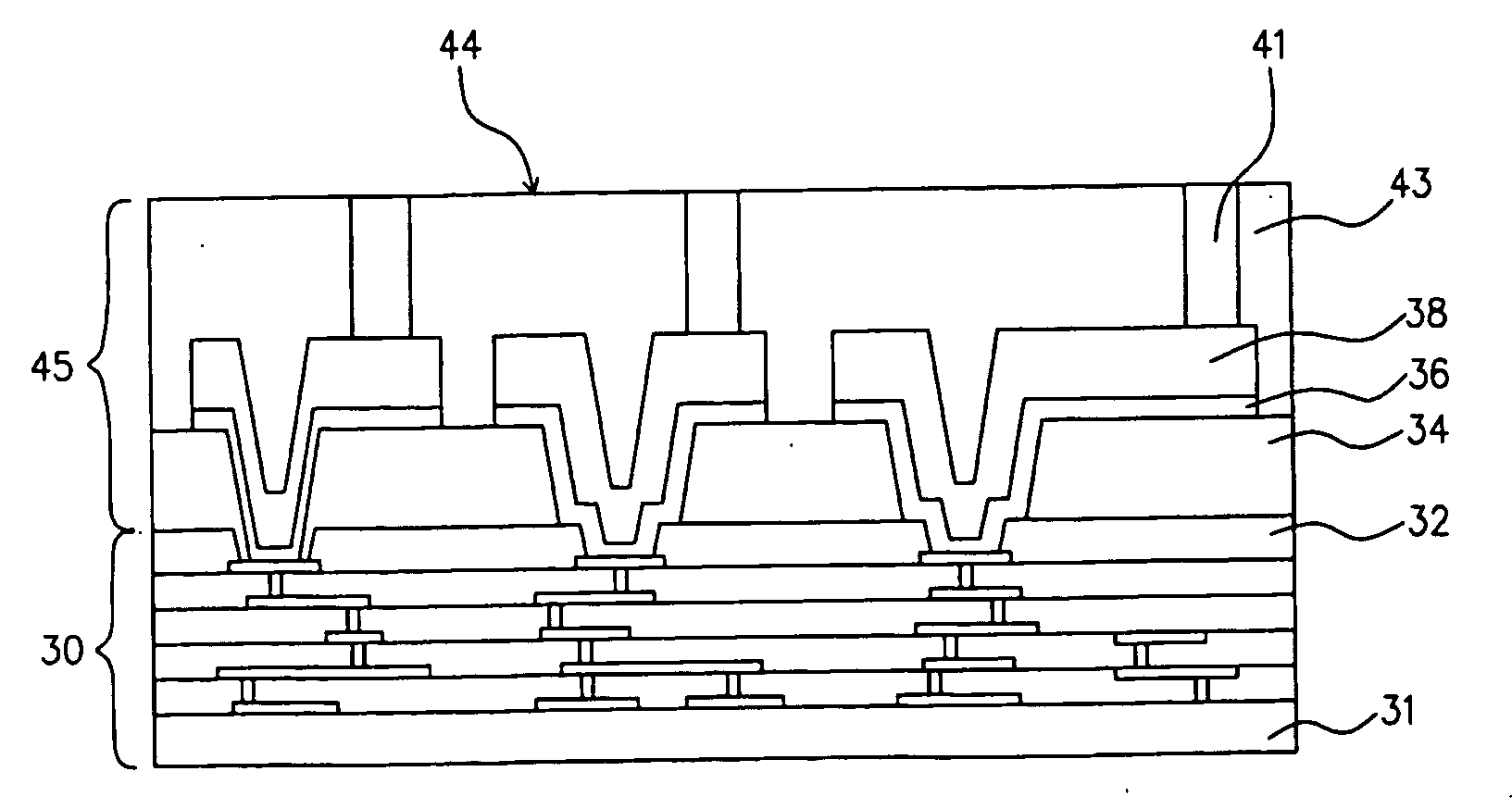
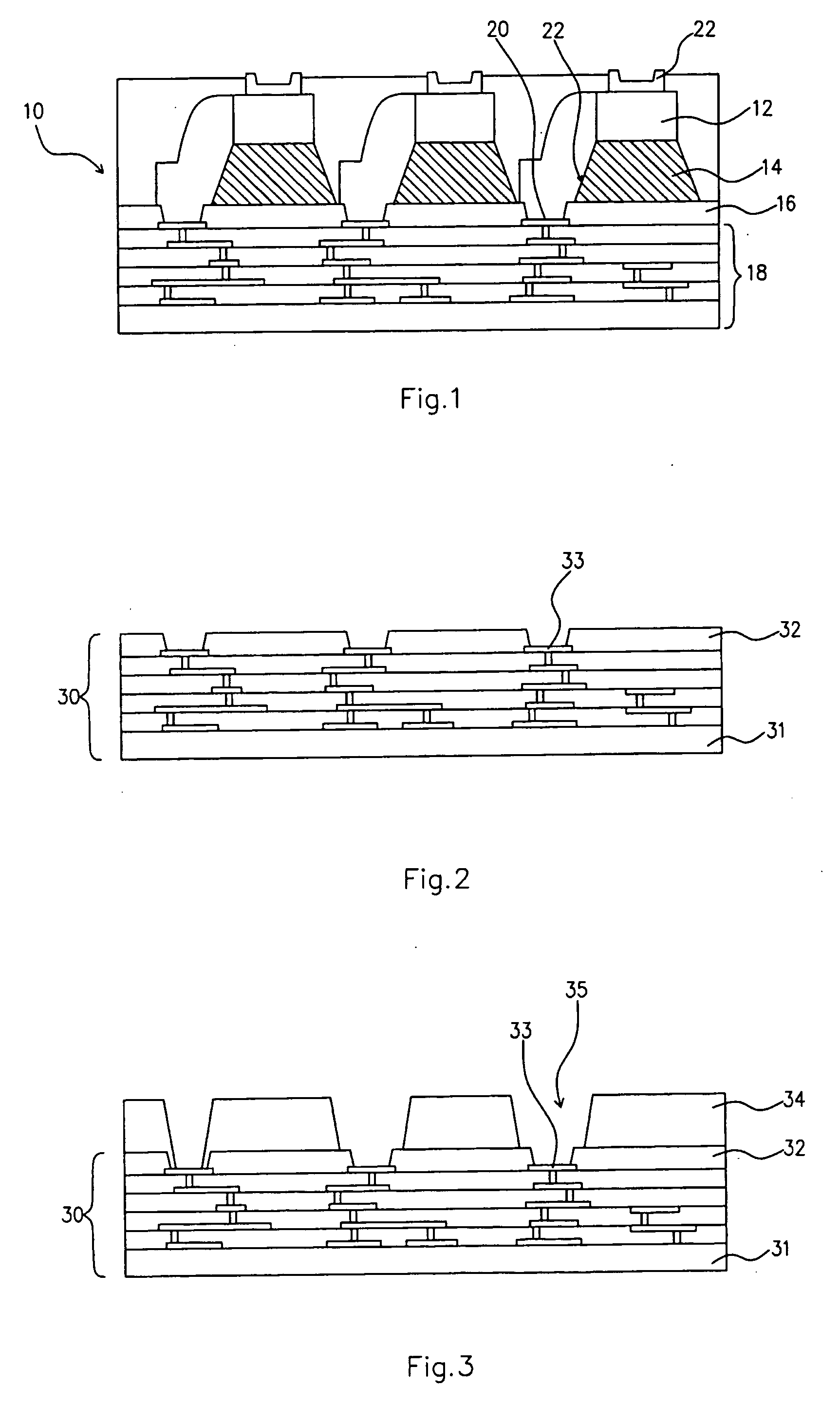
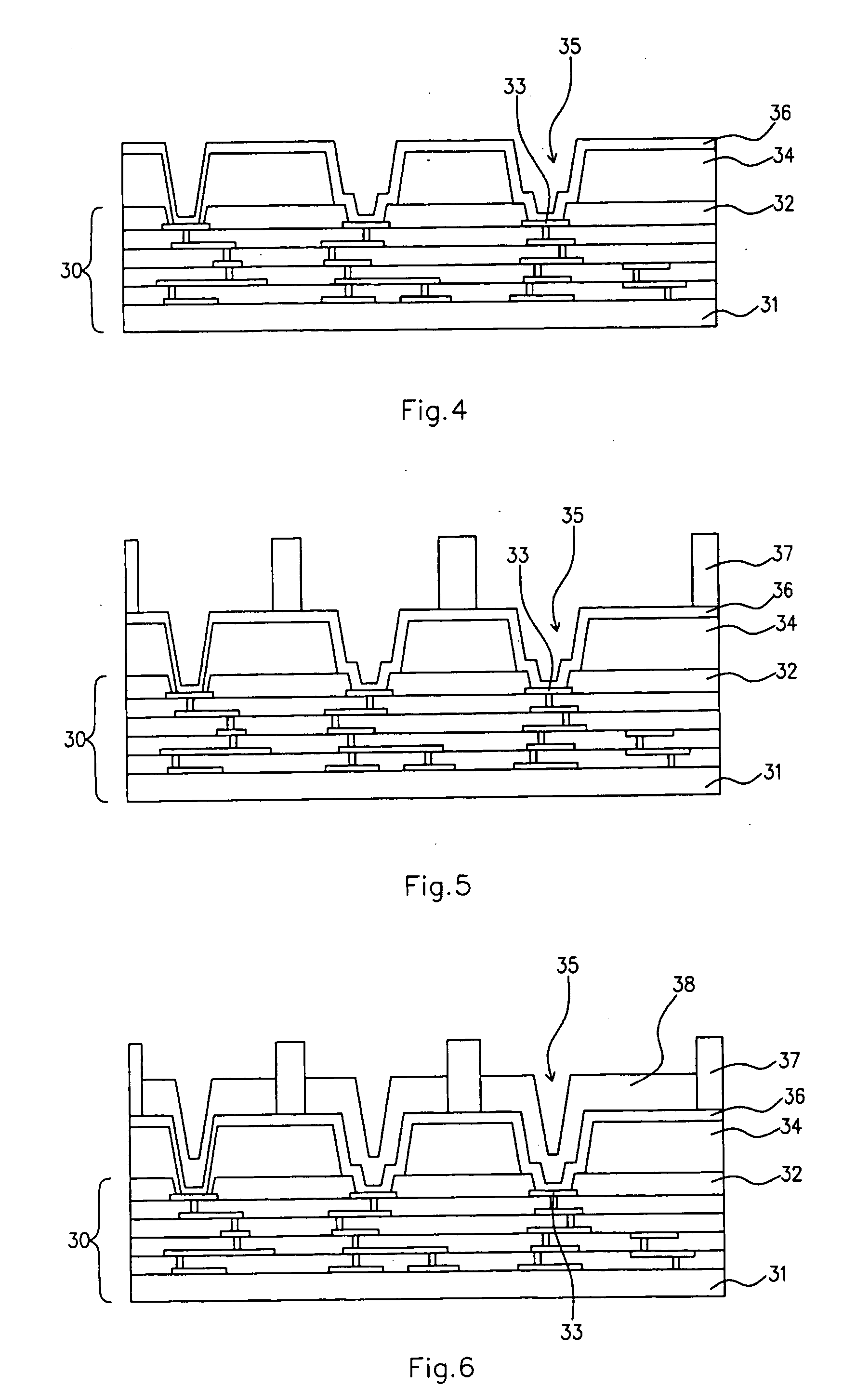
[0040] For purposes of illustrating the principles of the present invention and not by limitation, the present invention is described herein below by reference to structures and processes relating to WLP of IC chips. However, it is understood that the present invention is equally applicable to structures of other types of semiconductor devices, and other types of semiconductor pac...


PUM


Abstract

A post passivation rerouting support structure comprises a relatively thin support layer above the passivation layer to support the RDL, and a relatively thick support layer for fine pitch interconnects extending from the RDL and terminating as contact structures at the surface of the thick support layer, for a next level packaging structure. The thick support layer is planarized before defining the contact structures. The thick support layer may be formed after the conducting posts have been formed, or the thick support layer is formed before forming the conducting posts in vias formed in the thick support layer. An encapsulating layer may be provided above the thick support layer, which top surface is planarized before defining the contact structures. The encapsulating layer and the further support layer may be the same layer.

Description

INCORPORATION BY REFERENCE [0001] This application claims the priority of U.S. Provisional Application No. 60 / 678,525, filed May 6, 2005 and U.S. Provisional Application No. 60 / 693,549, filed Jun. 24, 2005. These documents are fully incorporated by reference as if fully set forth herein. [0002] The publications noted in the disclosure herein are each fully incorporated by reference, as if fully set forth in its entirety herein.BACKGROUND OF THE INVENTION [0003] 1. Field of the Invention [0004] The present invention relates to semiconductor devices, particularly to structures of semiconductor devices, and more particularly to post passivation structures for semiconductor devices and packaging processes for such. [0005] 2. Description of Related Art [0006] Semiconductor wafers are processed to produce IC (integrated circuit) chip having ever-increasing device density and shrinking feature geometries. Multiple conductive and insulating layers are required to enable the interconnection ...

Claims


Application Information

Patent Timeline
IPC IPC(8): G02B26/08
CPCH01L21/2885H01L21/563H01L21/76801H01L21/76885H01L23/3114H01L23/5223H01L23/5227H01L24/03H01L24/05H01L24/11H01L24/12H01L24/16H01L24/48H01L24/83H01L2224/0347H01L2224/0401H01L2224/04042H01L2224/04073H01L2224/05173H01L2224/05176H01L2224/05183H01L2224/05548H01L2224/05571H01L2224/05572H01L2224/05639H01L2224/05644H01L2224/05647H01L2224/05664H01L2224/05669H01L2224/1147H01L2224/13022H01L2224/13099H01L2224/131H01L2224/16H01L2224/45139H01L2224/45144H01L2224/45147H01L2224/48091H01L2224/48463H01L2224/83101H01L2224/83192H01L2924/01004H01L2924/01005H01L2924/01007H01L2924/01011H01L2924/01013H01L2924/01014H01L2924/01015H01L2924/01022H01L2924/01028H01L2924/01029H01L2924/01031H01L2924/01032H01L2924/01033H01L2924/01046H01L2924/01047H01L2924/0105H01L2924/01061H01L2924/01073H01L2924/01074H01L2924/01075H01L2924/01078H01L2924/01079H01L2924/01082H01L2924/01094H01L2924/014H01L2924/04941H01L2924/04953H01L2924/05042H01L2924/09701H01L2924/10329H01L2924/12044H01L2924/14H01L2924/19041H01L2924/19042H01L2924/19043H01L2924/30105H01L2924/30107H01L2924/3011H01L2924/01006H01L2924/01019H01L2924/01024H01L2924/01044H01L2924/01045H01L2924/01087H01L2224/48644H01L2224/48647H01L2224/48664H01L2224/48669H01L2224/48839H01L2224/48844H01L2224/48847H01L2224/48864H01L2224/48639H01L2924/13091H01L2924/00011H01L2924/1305H01L2924/00014H01L2924/0002H01L2924/00H01L2224/48869H01L2224/83851H01L2224/05552H01L2924/351H01L2924/15787H01L2924/15788H01L2224/45155H01L2224/45164H01L2224/45169H01L2224/45173H01L2224/45176H01L2224/45183H01L24/45H01L2224/05599H01L2224/45015H01L2924/207
Inventor LIN, MOU-SHIUNGCHOU, CHIEN-KANGCHEN, KE-HUNG
Owner QUALCOMM INC
Why Eureka
Try Eureka