Fabrication method of gallium manganese nitride single crystal nanowire

a gallium manganese nitride and single crystal technology, applied in the field of fabrication methods of gallium manganese nitride (gamnn) single crystal nanowires, can solve the problems of limited use of gallium nitride semiconductors, two-dimensional structures, and micrometer diameter gallium nitride semiconductors, and achieve the effects of increasing the number of nanowires, and increasing the cost of nanowires

Inactive Publication Date: 2006-12-28
KOREA INST OF SCI & TECH
View PDF6 Cites 19 Cited by
  • Summary
  • Abstract
  • Description
  • Claims
  • Application Information

AI Technical Summary

Problems solved by technology

However, as development of silicon semiconductors draws near to its limitation in principle, the world has now begun to turn to new-generation semiconductors aiming at diversification of technologies.
However, conventional gallium nitride semiconductors, having diameters of micrometer size and two-dimensional structures, are limited in their uses in electric and electronic nano devices which are becoming smaller and smaller.
Whereas researches on physical properties of nano particles and manufacture methods thereof are being carried actively, there are few manufacture methods of nanowire available.
However, this method is too complicated and requires a lot of time.
Moreover, the obt...

Method used


Image

  • Fabrication method of gallium manganese nitride single crystal nanowire
  • Fabrication method of gallium manganese nitride single crystal nanowire
  • Fabrication method of gallium manganese nitride single crystal nanowire

Examples


example

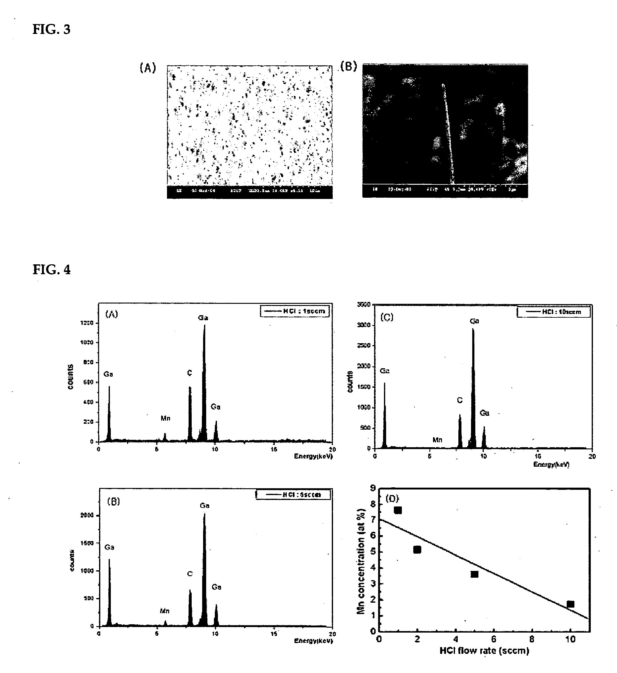
[0041] A (0001) sapphire substrate was washed with BOE (buffered oxide echant) to remove any native oxides, and then nickel (Ni) was deposited for 20 sec using a sputtering device. The nickel (Ni) was deposited as 2 nm-sized quantum dots. The sapphire substrate coated with nickel (Ni) was put in a horizontal tube furnace of 650° C. for 30 min to grow GaMnN single crystal nanowire. The tube was ¼ inch wide. Metallic Ga and metallic Mn were positioned with a spacing of 0.5 inch and 500 sccm of N2, 1 sccm of HCl gas and 20 sccm of ammonia (NH3) gas were injected. Of the 500 sccm of N2 gas, 200 sccm was used as diluent gas and 300 sccm was used as carrier gas.

[0042] Scanning electron micrographs were taken in order to confirm formation of the GaMnN single crystal nanowire. FIG. 3(A) is one at a magnitude of ×4.5 k (×4,500) and FIG. 3(B) is one of a single nanowire with the catalytic layer removed taken at a magnitude of ×20 k (×20,000).

[0043]FIG. 4 shows the change in the doping conce...


PUM

PropertyMeasurementUnit
Temperatureaaaaaaaaaa
Thicknessaaaaaaaaaa
Volume ratioaaaaaaaaaa

Abstract

The present invention relates to a fabrication method of gallium manganese nitride (GaMnN) single crystal nanowire, more particularly to a fabrication method of GaMnN single crystal nanowire substrate by halide vapor phase epitaxy (HVPE) in which such metal components as gallium (Ga) and manganese (Mn) react with such gas components as nitrogen (N2), hydrogen chloride (HCl) and ammonia (NH3), wherein the amount of the gas components are adjusted to control the Mn doping concentration in order to obtain nanowire having a perfect, one-dimensional, single crystal structure without internal defect, concentration of holes, or carriers, and magnetization value of which being determined by the doping concentration and showing ferromagnetism at room temperature, thus being a useful spin transporter in the field of the next-generation spintronics, such as spin-polarized LED, spin-polarized FET, etc.

Description

CROSS REFERENCE TO RELATED APPLICATION This application is based on, and claims priority from Korean Patent Application No. 10-2005-0055256, filed on Jun. 24, 2005, the disclosure of which is hereby incorporated by reference. TECHNICAL FIELD [0001] The present invention relates to a fabrication method of gallium manganese nitride (GaMnN) single crystal nanowire, more particularly to a fabrication method of GaMnN single crystal nanowire substrate by halide vapor phase epitaxy (HVPE) in which metal components such as gallium (Ga) and manganese (Mn) react with gas components such as nitrogen (N2), hydrogen chloride (HCl) and ammonia (NH3), wherein the amount of the gas components are adjusted to control the Mn doping concentration in order to obtain nanowire having a perfect, one-dimensional, single crystal structure without internal defect, concentration of holes, or carriers, and magnetization value of which being determined by the doping concentration and showing ferromagnetism at ...

Claims


Application Information

Patent Timeline
IPC IPC(8): C01B21/00
CPCB82Y30/00C01B21/0602C01P2002/85C01P2004/03C01P2004/16C04B2235/465C01P2004/64C01P2006/42C04B35/62286C04B2235/40C01P2004/62H01L21/20B82Y40/00
Inventor BYEUN, YUN-KIHAN, KYONG SOPSEONG, HAN KYUCHOI, HEON JINCHOI, SUNG CHURL
Owner KOREA INST OF SCI & TECH
Why Eureka
Try Eureka