Low temperature method for fabricating high-aspect ratio vias and devices fabricated by said method

a technology of throughwafer vias and low temperature, applied in the direction of semiconductor devices, semiconductor/solid-state device details, electrical apparatus, etc., can solve the problems of limited implementation of multi-technology circuits such as si cmos and sige, limited the implementation of integrated device circuits, and low-temperature methods. achieve the effect of enhancing chip performance, increasing the density of vias, and increasing circuitry

Active Publication Date: 2006-12-28
TELEDYNE SCI & IMAGING
View PDF19 Cites 81 Cited by
  • Summary
  • Abstract
  • Description
  • Claims
  • Application Information

AI Technical Summary

Benefits of technology

[0011] A feature of embodiments of the invention is the formation of small diameter through-substrate vias. An advantage of this feature is that a higher density of vias can be formed on a single substrate, thus allowing more circuitry to be included on a single substrate.
[0012] A further feature of embodiments of the invention is that the through-substrate vias can be fabricated at low temperatures. An advantage to this feature is that the formation of the vias does not damage circuitry contained within the substrate.
[0013] A still further feature of embodiments of the invention is that the activation of the isolation layer provides for conformal layers of conductive material. An advantage to this featur

Problems solved by technology

As the need for greater density of circuitry on a single substrate grew, the early simple planar chip designs proved inadequate.
Indeed, the planar designs limited the amount of circuitry that could be placed on a single substrate, and further limited the implementation of multi-technology circuits such as Si CMOS and SiGe, or integrated device circuits such as a MEMS device and a related control circuit.
Although three-dimensional chips using through-wafer vias have proven useful, they are currently limited.
In particular, one limitation is the inability to fabricate small-diameter, fine-pitch vias.
This limits the etch depth of the vias, and also reduces the amount of available space on the wafer for other uses.
Both dry etching and wet etching have been demonstrated for the thick wafer processing, and both suffer from constraints on via size and separation.
In addition, it is very difficult to reliably deposit electrical isolation layers and metallic conductors using low process temperature in the high aspect ratio vias.
In current systems the larger diameter vias are tolerated as ensuring the deposition of

Method used


Image

  • Low temperature method for fabricating high-aspect ratio vias and devices fabricated by said method
  • Low temperature method for fabricating high-aspect ratio vias and devices fabricated by said method
  • Low temperature method for fabricating high-aspect ratio vias and devices fabricated by said method

Examples


Embodiment Construction

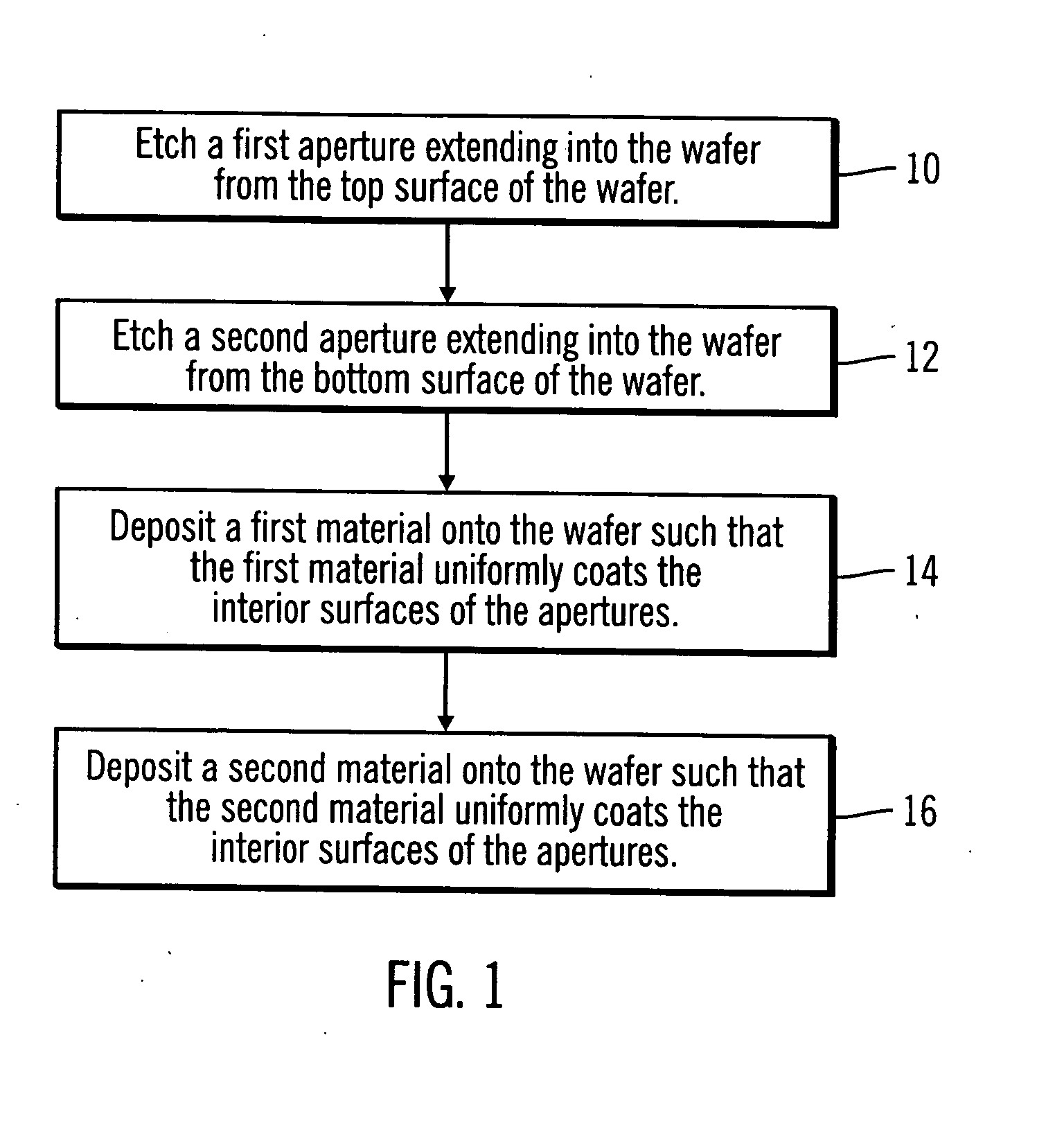
[0021] Embodiments of the present invention are directed to a process for fabricating high aspect ratio through-wafer vias at low temperatures. The fabrication process produces high performance silicon chips or CMOS assemblies having high density via interconnects.

[0022] With reference to FIG. 1, in preferred embodiments, to form a via, a first cavity is etched into the first surface of a wafer 10. After the first cavity is formed, a second cavity is etched into the second surface of the wafer 12. Once the first and second cavities are formed, a first material is deposited onto the wafer such that it uniformly coats the wafer 14, including uniformly coating the interior walls of the cavities. Finally, a second material is deposited onto the wafer such that the second material uniformly coats the wafer 16, including the interior walls of the cavity.

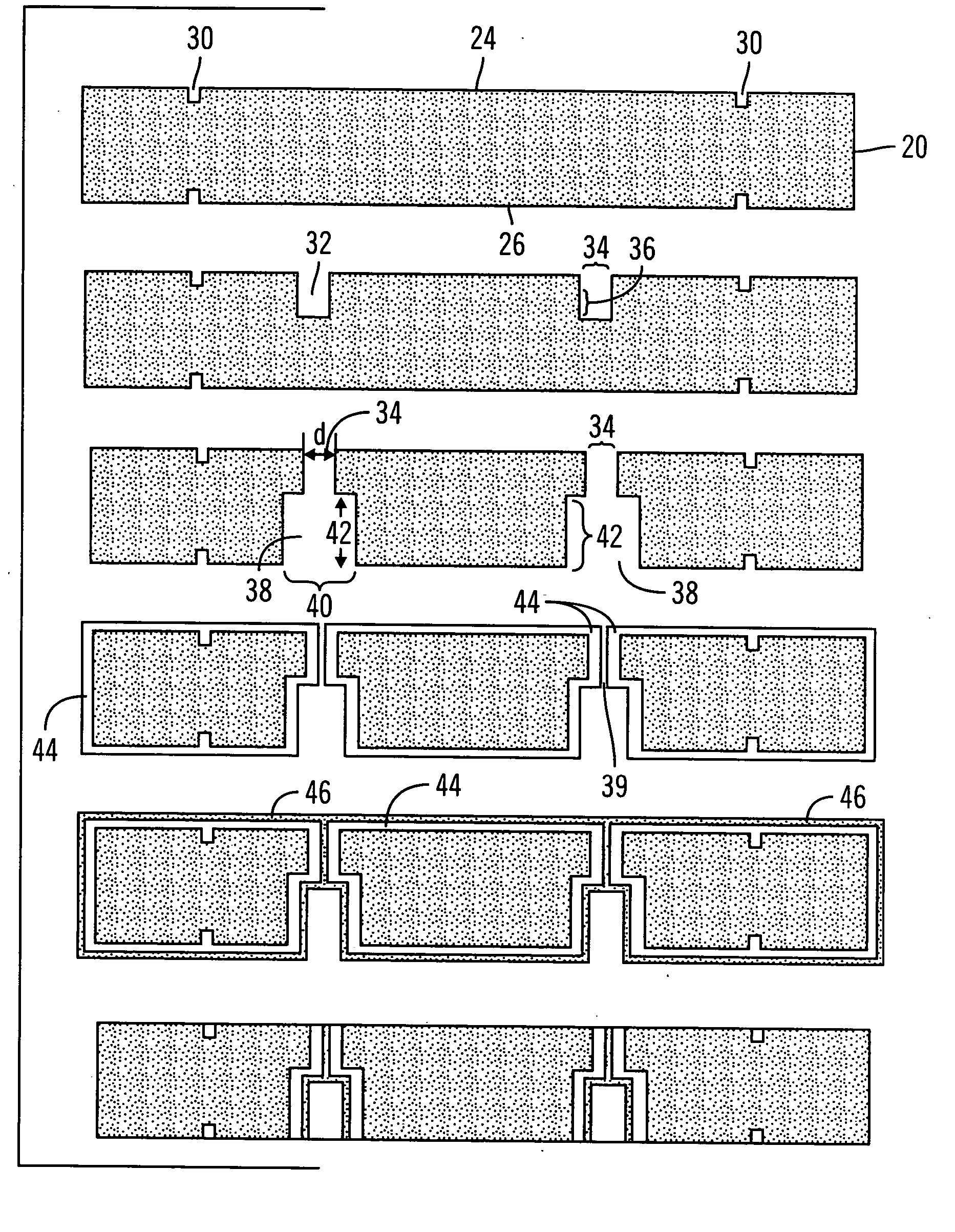
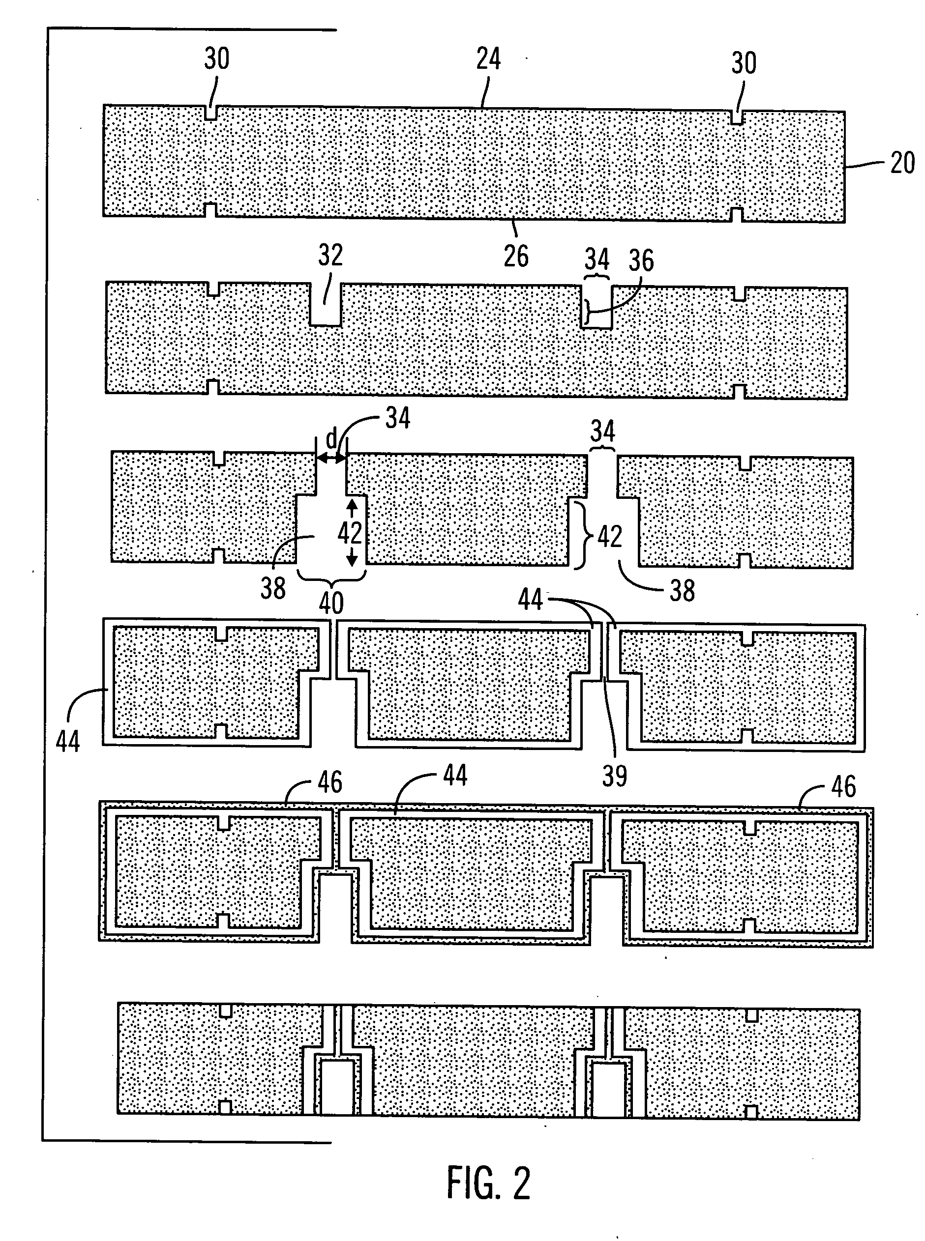
[0023] With reference to FIG. 2, the wafer 20, also referred to as a substrate, comprises a first surface 24, a second surface 26 and a...


PUM


Abstract

Embodiments of the present invention are directed to a process for forming small diameter vias at low temperatures. In preferred embodiments, through-substrate vias are fabricated by forming a through-substrate via; and depositing conductive material into the via by means of a flowing solution plating technique, wherein the conductive material releases a gas that pushes the conductive material through the via to facilitate plating the via with the conductive material. In preferred embodiments, the fabrication of the substrate is conducted at low temperatures.

Description

FIELD OF THE INVENTION [0001] This invention is directed to a method for fabricating high-aspect ratio through-wafer vias. In particular, embodiments of the invention are directed to methods for the low temperature fabrication of through-wafer vias having small diameters. The invention is also directed to devices fabricated using such methods. BACKGROUND [0002] The fabrication of integrated circuit chips has become a sophisticated process that can allow complex circuitry to be densely packaged onto a single wafer, also known as a substrate. Originally, most chips were fabricated in a simple planar design. As the need for greater density of circuitry on a single substrate grew, the early simple planar chip designs proved inadequate. Indeed, the planar designs limited the amount of circuitry that could be placed on a single substrate, and further limited the implementation of multi-technology circuits such as Si CMOS and SiGe, or integrated device circuits such as a MEMS device and a ...

Claims


Application Information

Patent Timeline
IPC IPC(8): H01L21/76H01L21/44
CPCH01L21/288H01L21/76898H01L23/481H01L2924/0002H01L2924/00
Inventor BORWICK, ROBERT L.STUPAR, PHILIP A.DENATALE, JEFFREY F.TSAI, CHAILUNYAO, ZHIMIN J.GARRETT, KATHLEENWHITE, JOHNWARREN, LESTENCH, MORGAN
Owner TELEDYNE SCI & IMAGING
Why Eureka
Try Eureka