Semiconductor device and method for manufacturing the same

a semiconductor and semiconductor technology, applied in the direction of solid-state devices, transistors, instruments, etc., can solve the problems of inability to avoid reading errors due to manual operation of bar code reading, inefficient information management through bar codes, and limited information that can be provided, so as to achieve convenient operation, shorten the time, and not spoil

Inactive Publication Date: 2007-01-04
SEMICON ENERGY LAB CO LTD
View PDF11 Cites 20 Cited by
  • Summary
  • Abstract
  • Description
  • Claims
  • Application Information

AI Technical Summary

Benefits of technology

[0023] Information exchange or information management can be conducted more easily in a shorter time by using a thin film integrated circuit according to the present invention than by using an information supplying means such as bar codes, and thus, a wide variety of information can be provided. Further, a thin film integrated circuit according to the present invention is extremely thin unlike a conventional silicon wafer, and therefore, the design is not spoilt when it is attached to a product or the like.
[0024] The cost of a chip, i.e. an ID chip can be lowered as compared with a chip of a conventional silicon wafer, since the ID chip is formed over a glass substrate or the like. A chip formed by using a silicon wafer has a limitation on a shape of a mother substrate, since it is taken out a circular silicon wafer. On the other hand, an ID chip according to the present invention has no limitations on a shape of a mother substrate, since the mother substrate is an insulating substrate such as glass. Accordingly, the productivity can be enhanced and mass-production is possible. As a result, further cost reduction can be expected. An integrated circuit having extremely low unit cost such as a chip of the present invention generates enormous profits by reducing the unit cost.

Problems solved by technology

When the information management is performed by using bar codes, the amount of information that can be provided is limited according with such increase in information.
Information management by using bar codes is inefficient since it spends time for reading manually.
Further, reading errors due to the manual operation of bar code reading cannot be avoided.
An IC card is more expensive than a magnetic card, and an electronic tag is also more expensive as a substitute for bar codes.
As a result, diffusion thereof is prevented, and the IC card and the electronic tag are limited to an application having an important added value.
Concerning Reference 1, there are problems that consumers take a lot of labor to access the Internet and that they must have their own personal computers or the like.
Further, in References 1 and 2, unevenness is produced on the surface of merchandise or a product since the integrated circuit including a silicon wafer is thick, in the case where the integrated circuit is mounted in the merchandise or the product, in particular, a paper such as a bill or a label itself attached to the merchandise or the product.

Method used


Image

  • Semiconductor device and method for manufacturing the same
  • Semiconductor device and method for manufacturing the same
  • Semiconductor device and method for manufacturing the same

Examples


embodiment mode 1

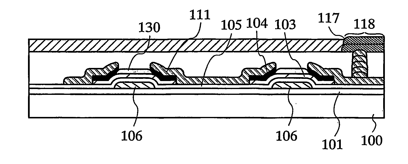
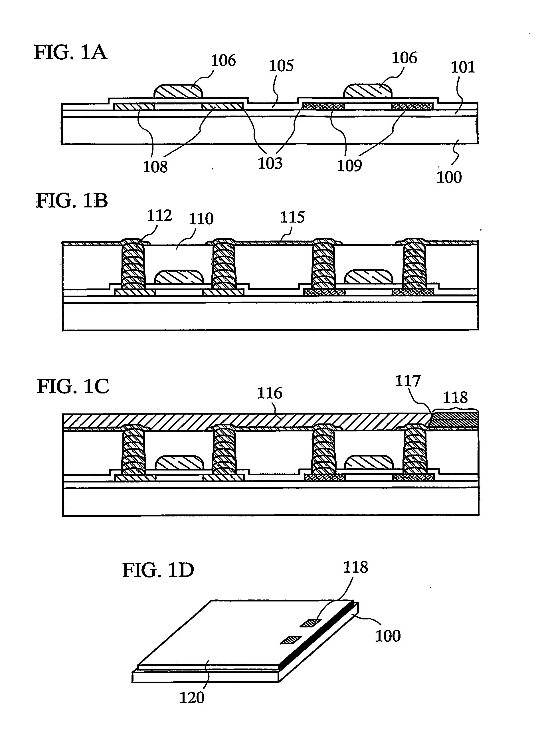
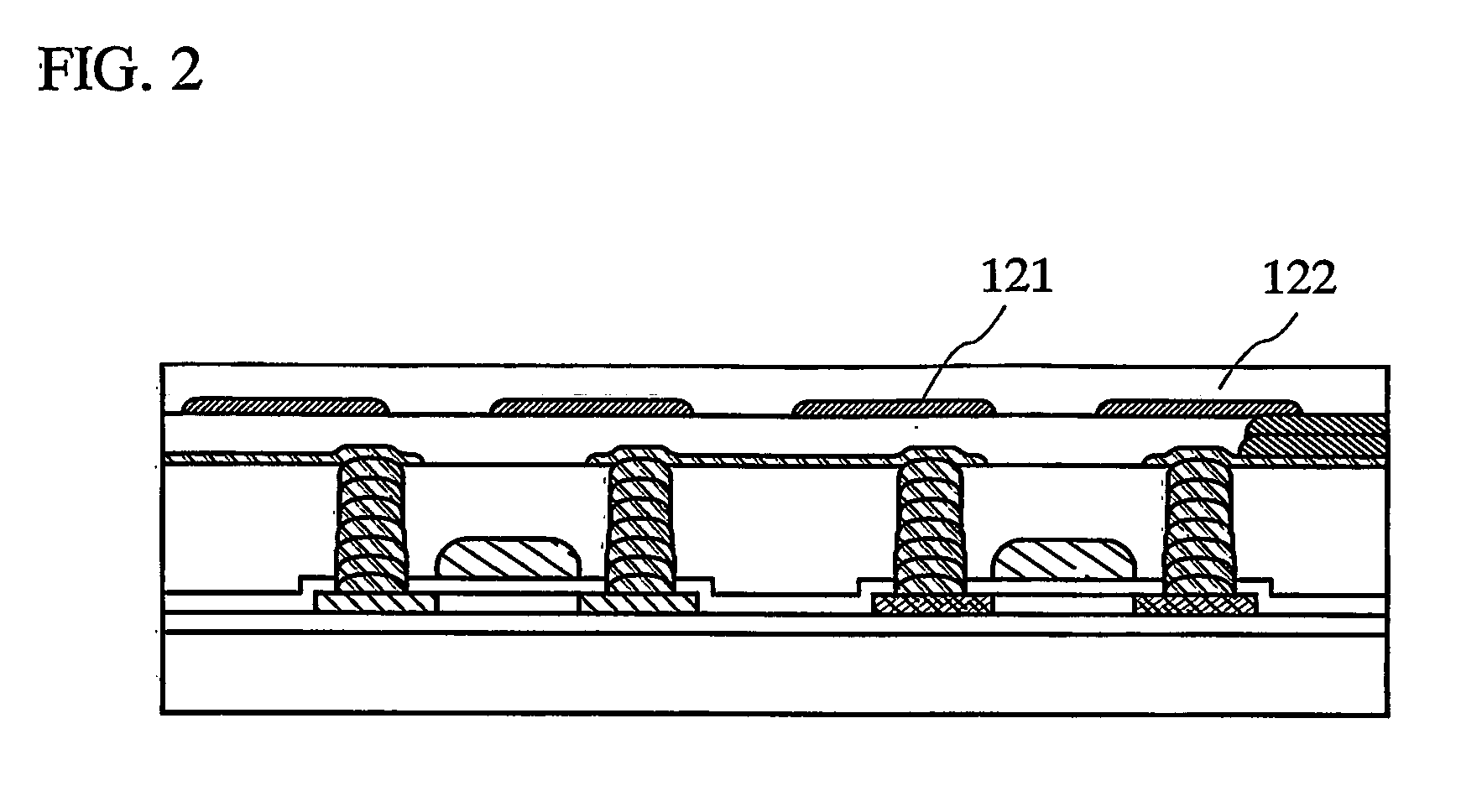
[0043] Embodiment Mode 1 describes an example of a method of manufacturing a thin film integrated circuit to be mounted in an ID chip.

[0044] As shown in FIG. 1A, a substrate 100 having an insulating surface is prepared. For example, a glass substrate such as a barium borosilicate glass or an alumino borosilicate glass, a quartz substrate, a stainless substrate or the like can be used for the substrate 100. In addition, a substrate comprising plastic typified by polyethylene-terephthalate (PET), polyethylene naphthalate (PEN), polyeter sulfone (PES) and a substrate made of synthetic resin having flexibility such as acryl generally tend to have worse heat-resistance than other types of substrates. However, such substrates can be used as long as they can resist a treatment temperature in a manufacturing step.

[0045] In order to enhance the planarity of the substrate, the substrate is preferably used after the surface thereof is polished by a chemical or mechanical polishing method, a ...

embodiment mode 2

[0091] Embodiment Mode 2 describes a method for manufacturing a thin film integrated circuit provided with a thin film transistor having a non-crystalline semiconductor film, unlike the above described embodiment mode.

[0092] As in the above described embodiment mode, a substrate having insulating surface 100 is prepared as shown in FIG. 3A. A material of the substrate having insulating surface can be referred to the above described embodiment mode. In this embodiment mode, a heat treatment for crystallizing is not required since the semiconductor film is non-crystalline. Consequently, a substrate of synthetic resin having flexibility is easy to be employed.

[0093] As in the above embodiment, a surface polishing may be conducted on the substrate having insulating surface so as to enhance its planarity.

[0094] After that, a base film 101 is formed. A manufacturing method or a material of the base film may be referred to the above described embodiment mode. A conductive film such as t...

embodiment mode 3

[0124] A thin film integrated circuit manufactured by a method different from that of the embodiment mode described above is described in Embodiment Mode 3. This embodiment mode describes the thin film transistor shown in Embodiment Mode 1, but the thin film transistor shown in Embodiment Mode 2 may be also used.

[0125] As shown in FIG. 5A, a metal film 140 is formed over a substrate 100. The metal film can be formed of a single layer of an element selected from W, Ti, Ta, Mo, Nd, Ni, Co, Zr, Zn, Ru, Rh, Pd, Os, and Ir, an alloy material or a compound material, each of which is mainly containing these elements; or a lamination layer thereof. As a method for forming the metal film, a sputtering method using a target of a metal may be employed, for example. The metal film may be formed to have a thickness of from 10 to 200 nm, preferably, from 50 to 75 nm.

[0126] Instead of the metal film, a film of such a metal which is nitrided (for example, nitride tungsten or nitride molybdenum) c...


PUM


Abstract

An IC card is more expensive than a magnetic card, and an electronic tag is also more expensive as a substitute for bar codes. Therefore, the present invention provides an extremely thin integrated circuit that can be mass-produced at low cost unlike a chip of a conventional silicon wafer, and a manufacturing method thereof. One feature of the present invention is that a thin integrated circuit is formed by a formation method that can form a pattern selectively, on a glass substrate, a quartz substrate, a stainless substrate, a substrate made of synthetic resin having flexibility, such as acryl, or the like except for a bulk substrate. Further, another feature of the present invention is that an ID chip in which a thin film integrated circuit and an antenna according to the present invention are mounted is formed.

Description

TECHNICAL FIELD [0001] The present invention relates to a chip comprising a paper-like thin film integrated circuit, which has a memory or the like, and merchandises or products to which a label using the chip is attached, and further a method for manufacturing thereof. BACKGROUND ART [0002] In recent years, one person possesses many cards. The amount of information has been kept increasing since various kinds of information are stored in a card and rewritten as necessary. [0003] The increase in the amount of information is essential in many fields. For example, there are heightened calls for strengthening product safety or management system to the food industry or the manufacturing industry, and thus, product information is increased. However, the current products information is exceedingly little, as information such as a country of manufacture, a maker, a product number which are mainly provided by using bar codes containing figures of over ten columns. Further, when bar codes ar...

Claims


Application Information

Patent Timeline
Patent Type & Authority Applications(United States)
IPC IPC(8): H01L21/84H01L31/113G06K19/077H01L21/336H01L21/77H01L27/12H01L27/13H01L29/786
CPCG06K19/07749H01L27/12H01L27/13H01L29/66757H01L27/1292H01L29/78603H01L29/78684H01L27/1285H01L29/66765
Inventor MAEKAWA, SHINJIFUJII, GENMARUYAMA, JUNYATAKAYAMA, TORUFUKUMOTO, YUMIKOARAI, YASUYUKI
Owner SEMICON ENERGY LAB CO LTD
Why Eureka
Try Eureka