Nanoparticle thin film, method for dispersing nanoparticles and method for producing nanoparticle thin film using the same

Inactive Publication Date: 2007-01-11
SAMSUNG ELECTRONICS CO LTD
View PDF3 Cites 30 Cited by
  • Summary
  • Abstract
  • Description
  • Claims
  • Application Information

AI Technical Summary

Benefits of technology

[0020] Example embodiments of the present invention provide a method for dispersing nanoparticles by which defects

Problems solved by technology

Aggregations may not sufficiently exhibit their inherent advantages.
When modifying the surface of nanoparticles by sonication, instability problems (e.g., destruction of the nanoparticles) may occur.
Over longer periods of time, higher ultrasonic energy used during sonication may result in increased destruction and defects of the nanoparticles.
If the reaction time is shortened in order to reduce the defects, the reaction may not proceed sufficiently and the yield may be lower.
According to a conventional separation process wherein aggregated particles may be removed from sonicated nanoparticles using a column or a filter, because nanoparticles may be passed through a filter having smaller pores, a higher water pressure may be applied to the filter for a longer time and the nanoparticles may adsorb onto the filter, leading to a loss of the nanoparticles.
Accordingly, these separation processes may be unsuitable for the prod

Method used


Image

  • Nanoparticle thin film, method for dispersing nanoparticles and method for producing nanoparticle thin film using the same
  • Nanoparticle thin film, method for dispersing nanoparticles and method for producing nanoparticle thin film using the same
  • Nanoparticle thin film, method for dispersing nanoparticles and method for producing nanoparticle thin film using the same

Examples


example 1

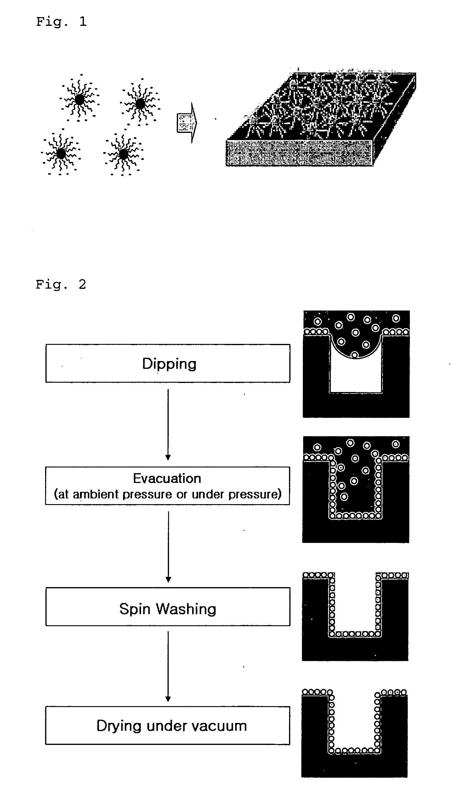
Dispersion of Nanoparticles

[0092] 1.8424 g of mercaptoacetic acid (MAA) may be dissolved in 8 ml of chloroform and then the solution may be heated to about 70° C. 3 ml of CdSe nanoparticles may be slowly added to the solution at 70° C. while rapid stirring. The mixture may be reacted while stirring under reflux conditions at about 70° C. for approximately 3 hours. After completion of the reaction, the reaction mixture may be centrifuged at approximately 3,000 rpm to obtain a precipitate. The precipitate may be dispersed in chloroform and centrifuged at about 3,000 rpm for approximately 5 minutes. The dispersion and / or centrifugation may be repeated about seven times. The washed nanoparticles may be dried under vacuum for about 6 hours, and dispersed in a Tris buffer (0.1M, pH=9). The dispersion may be centrifuged at about 15,000 g for approximately 10 minutes to reduce nanoparticle aggregates.

example 2

Production of 2-Dimensional Monolayer Nanoparticle Thin Film

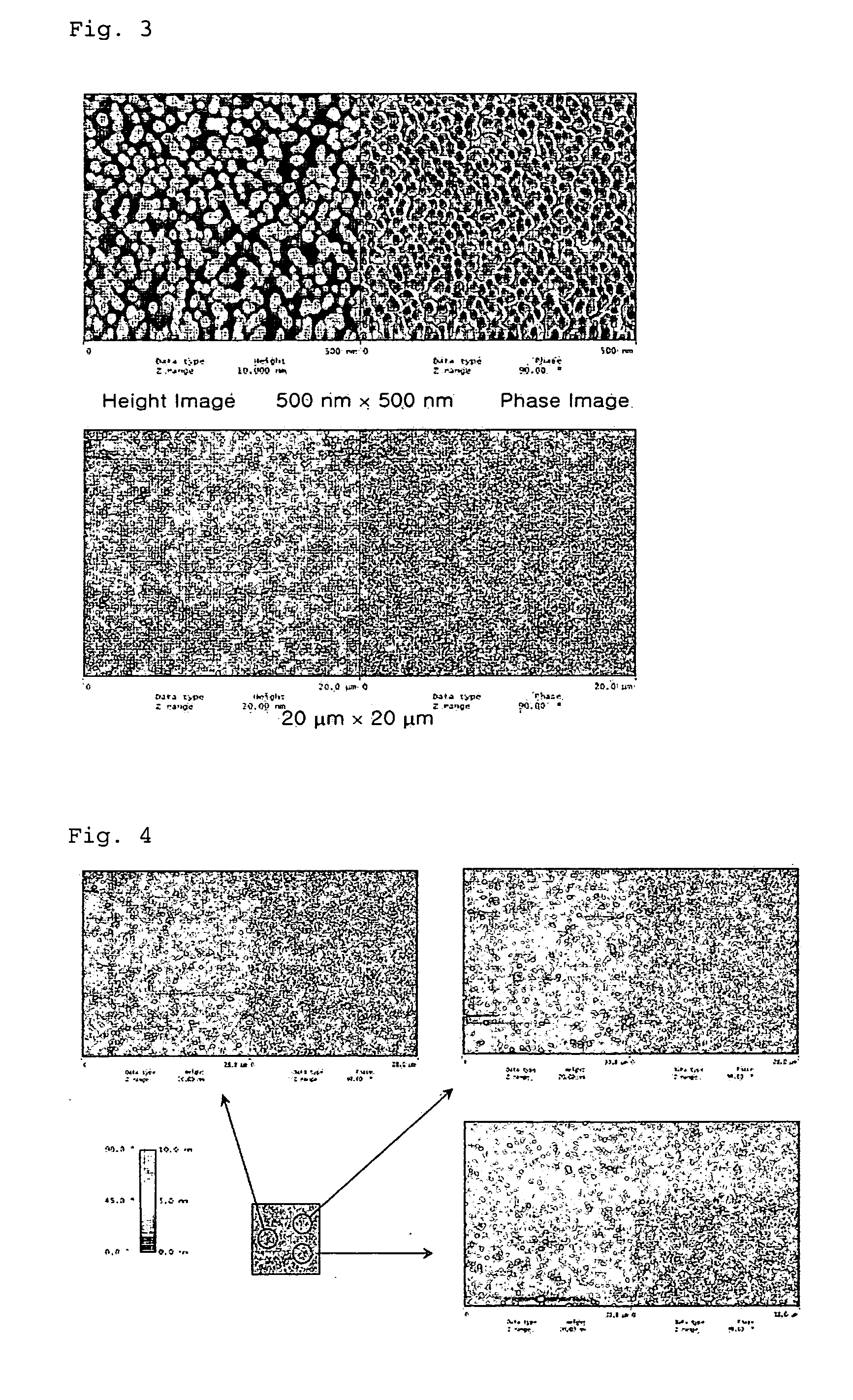
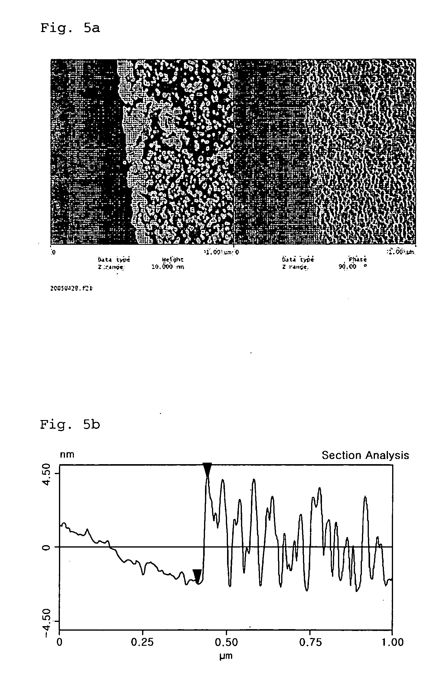
[0093] A 12-inch silicon wafer substrate may be placed in a pirana solution (H2SO4 / H2O2=1 / 3 (v / v), heated for approximately 15 minutes, and washed with methanol / toluene. The washed substrate may be subjected to sonication in an RCA solution (NH4OH / H2O2 / H2O=1 / 1 / 5) at about 70° C. for approximately one hour, followed by sonication in methanol. Subsequently, the sonicated substrate may be dipped in a solution of an aminosilane (5% by volume) in toluene to react for approximately 5 hours to adsorb an amine group to the substrate surface, washed with deionized water, and dried. The dried substrate may be dip-coated with the nanoparticle dispersion prepared in Example 1 for approximately one hour, washed, and dried to form a thin film. The atomic force microscopy images of the nanoparticle thin film may be obtained using a nanoscope IV (Digital Instrument). The images may resemble those shown in FIGS. 3 to 5.

[0094]FIG. 3 shows ...

example 3

Production of 3-Dimensional Monolayer Nanoparticle Thin Film of 400 nm (Diameter)×400 nm (Depth)

[0098] A 12-inch silicon wafer substrate of about 400 nm (diameter)×400 nm (depth) may be placed in a pirana solution (H2SO4 / H2O2=1 / 3 (v / v), heated for approximately 15 minutes, and washed with methanol / toluene. The washed substrate may be subjected to sonication in an RCA solution (NH4OH / H2O2 / H2O=1 / 1 / 5) at about 70° C. for approximately one hour, followed by sonication in methanol. Subsequently, the sonicated substrate may be dipped in a solution of an aminosilane (5% by volume) in toluene to react for approximately 5 hours to adsorb an amine group to the substrate surface, and spun at about 3,000 rpm for approximately 5 seconds to remove the reaction solution by centrifugal force. The resulting substrate may be dipped in deionized water for 5 seconds and washed by spinning at about 3,000 rpm. The washed substrate may be stored in an aqueous HCl solution (pH=1) before use. Subsequently,...


PUM

PropertyMeasurementUnit
Temperatureaaaaaaaaaa
Timeaaaaaaaaaa
Timeaaaaaaaaaa

Abstract

A nanoparticle thin film, a method for dispersing nanoparticles and a method for producing nanoparticle thin film using the same. The method for dispersing nanoparticles may include modifying the surface of nanoparticles with a charged material, drying the surface-modified nanoparticles under vacuum and/or dispersing the dried nanoparticles in a solvent. According to the methods provided, the nanoparticle thin film may exhibit more stability, lesser defects and/or lesser aggregation of nanoparticles. In addition, 2-dimensional and/or 3-dimensional nanoparticle thin films may be produced in which nanoparticles may be more uniformly applied over larger areas. The nanoparticle thin films produced by the methods may be more effectively used for a variety of applications (e.g., flash memory devices, DRAMs, hard disks, luminescent devices, organic light-emitting diodes (OLEDs) or the like).

Description

PRIORITY STATEMENT [0001] This non-provisional application claims priority under 35 U.S.C. § 119 (a) on Korean Patent Applications No. 2005-60215 filed on Jul. 5, 2005, No. 2005-101361 filed on Oct. 26, 2005 and No. 2006-3661 filed on Jan. 12, 2006, both of which are herein incorporated by reference in their entirety. BACKGROUND OF THE INVENTION [0002] 1. Field of the Invention [0003] Example embodiments of the present invention relate to a nanoparticle thin film, a method for dispersing nanoparticles and a method for producing a nanoparticle thin film using the same. Other example embodiments of the present invention relate to a method for dispersing nanoparticles by modifying the surface of nanoparticles with a charged material, drying the surface-modified nanoparticles under vacuum, dispersing the dried nanoparticles in a solvent and / or centrifuging to prepare a dispersion of the nanoparticles. Example embodiments of the present invention also relates to a method for producing a ...

Claims


Application Information

Patent Timeline
IPC IPC(8): H01L29/08B32B19/00H01L51/00C09K23/00
CPCB05D1/00B05D3/0493Y10T428/29B82Y30/00B82Y40/00B05D3/10A41C3/12A41F1/006A44B13/0052A41C3/02
Inventor CHOI, JAE YOUNGCHO, KYUNG SANGYOON, SEON MILEE, EUN SUNGLEE, JAE HO
Owner SAMSUNG ELECTRONICS CO LTD
Why Eureka
Try Eureka