Hole transport material for organic electroluminescence devices and organic electroluminescence device using the same

a technology of electroluminescence devices and transport materials, which is applied in the direction of solid-state devices, discharge tubes/lamp details, natural mineral layered products, etc., can solve the problems of inadequate improvement of carrier injection barrier at interface, inadequate driving voltage of devices, and insufficient carrier mobility of hole transport materials, etc., to achieve excellent hole transporting properties, improve hole mobility, and improve the effect of transporting properties

Inactive Publication Date: 2007-01-11
SANYO ELECTRIC CO LTD
View PDF6 Cites 10 Cited by
  • Summary
  • Abstract
  • Description
  • Claims
  • Application Information

AI Technical Summary

Benefits of technology

[0016] The bulk resistance is represented as values of specific resistance, and the specific resistance may be reduced by enhancing an electrical conductivity which is the reciprocal of the specific resistance. The electrical conductivity is represented as the product of the carrier concentration, the charge and the mobility, and a material having higher mobility exhibits a higher electrical conductivity and can reduce the specific resistance. That is, it is essential to develop a highly electrically conductive or highly mobile material in order to reduce the bulk resistance.
[0038] The hole transport material for organic EL devices of the present invention consists of a copolymer having a first unit consisting of a heterocyclic compound containing a sulfur atom and a second unit consisting of a secondary or tertiary amine compound. Since these units take on a structure having an excellent hole transporting property and the copolymer of the present invention has both of such the units, the hole transport material for organic EL devices of the present invention exhibits a more excellent hole transporting property by a synergistic effect of these units. Accordingly, by using the hole transport material of the present invention for the organic EL devices, the hole mobility can be improved and the driving voltage of the organic EL device can be reduced.

Problems solved by technology

However, in theses prior arts, the driving voltages of the device were not adequately low, though their characteristics had been improved.
The reason for this is that the carrier mobility of the hole transport material and the barrier of carrier injection at an interface, which is inherent to the organic EL device, were not improved adequately.

Method used


Image

  • Hole transport material for organic electroluminescence devices and organic electroluminescence device using the same
  • Hole transport material for organic electroluminescence devices and organic electroluminescence device using the same
  • Hole transport material for organic electroluminescence devices and organic electroluminescence device using the same

Examples


experiment 1

[Experiment 1]

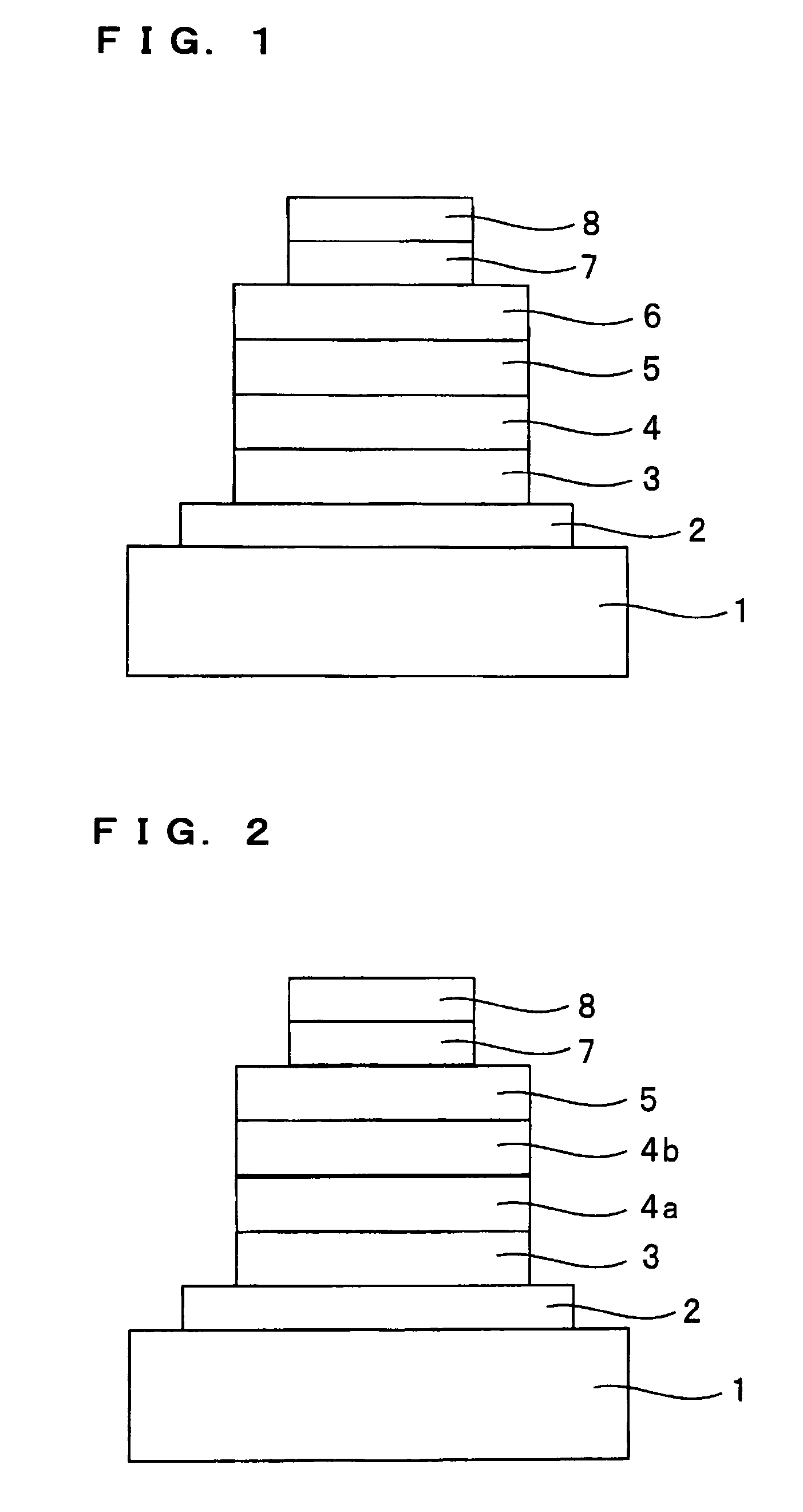
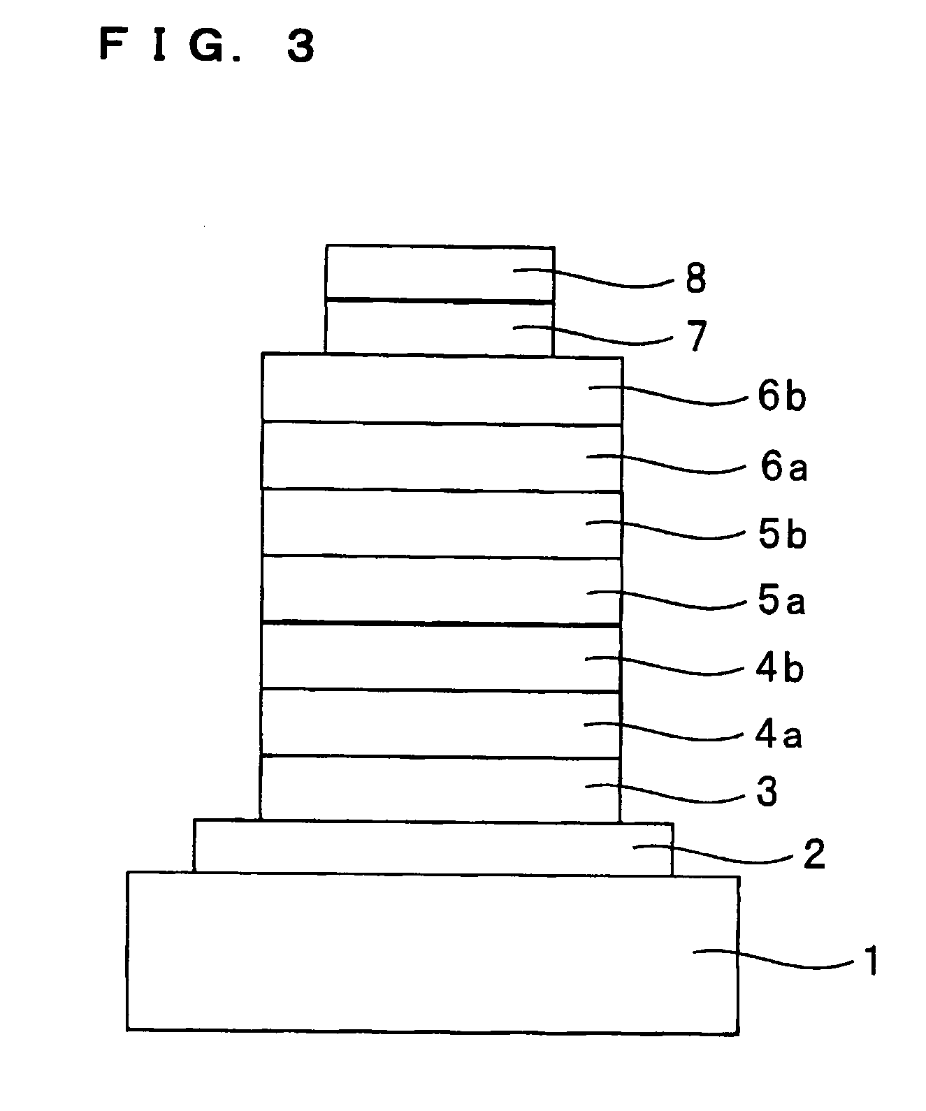
[0077] In Examples 1 to 7 and Comparative Example 1, each organic EL device having a structure shown in FIG. 2 was prepared in the following manner.

example 1

[0078] A copolymer PF8-tBuTPD-Th according to the present invention was synthesized by following the procedure described below.

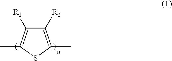
[0079] A reaction apparatus equipped with a stirrer was dried well and connected to a nitrogen line / a vacuum line. Into this reactor were charged 48.4 mg (0.2 mmol) of 2,5-dibromothiophene, 227.4 mg (0.3 mmol) of N,N′-bis(4-bromophenyl)-N,N′-bis(4-tert-butylphenyl)-benzidine, 321 mg (0.5 mmol) of 9,9-dioctylfluorene-2,7-bis(4,4,5,5-tetramethyl-1,3,2-dioxaborolan), a catalyst for Suzuki coupling reaction, 5 ml of toluene and 8 ml of a basic aqueous solution. After plugging an opening of the reactor with a rubber stopper, by repeating short-time evacuation and N2 purge three times, air in the reactor was replaced with nitrogen gas and a solvent was degassed. Then, the reactor was heated to 90° C. and a reaction was continued for about 3 hours in an atmosphere of nitrogen while keeping the reactor at 90° C. Then, 61 mg (0.5 mmol) of phenylboronic acid was adde...

example 2

[0084] An organic EL device was prepared by following the same procedure as in Example 1 except for providing a second hole transport layer 4b consisting of NPB having a film thickness of 30 nm on a first hole transport layer 4a and providing an emission layer 5 on the second hole transport layer 4b.


PUM

PropertyMeasurementUnit
emission luminanceaaaaaaaaaa
peak wavelengthaaaaaaaaaa

Abstract

A hole transport material for organic electroluminescence devices, characterized by consisting of a copolymer having a first unit consisting of a heterocyclic compound containing a sulfur atom and a second unit consisting of a secondary or tertiary amine compound, wherein the above-mentioned hole transport material preferably further includes a third unit having a conjugated structure, preferably uses a thiophene derivative as the heterocyclic compound of the first unit, preferably uses a diphenylamine derivative and a triphenylamine derivative as the secondary or tertiary amine compound of the second unit, and includes a structure of a fluorene derivative or a structure of a phenylene derivative as the third unit, and an organic electroluminescence device using the same.

Description

[0001] The priority Japanese Patent Application Number 2005-54149 upon which this patent application is based is hereby incorporated by reference. BACKGROUND OF THE INVENTION [0002] 1. Field of the Invention [0003] The present invention relates to a hole transport material for organic electroluminescence devices and an organic electroluminescence device using the same. [0004] 2. Description of the Related Art [0005] In recent years, as information equipment is diversified, needs for flat display devices, of which the power consumption is lower than that of CRT (cathode ray tube) commonly used, have sharply increased. As one of the flat display devices, organic electroluminescence devices (organic EL devices) which have features such as high efficiency, a low-profile, a light weight and low viewing angle dependence receive attention. [0006] Particularly in a driving voltage, while an inorganic EL device, the same EL device, needs a high voltage of several dozen V or higher, an organi...

Claims


Application Information

Patent Timeline
Patent Type & Authority Applications(United States)
IPC IPC(8): C08G61/12H01L51/54H05B33/14
CPCC08G61/02H05B33/14C08G61/12C08G61/126C08G73/026C09K11/06C09K2211/1007C09K2211/1011C09K2211/1037H01L51/0036H01L51/0039H01L51/0043H01L51/0054H01L51/0055H01L51/0058H01L51/0059H01L51/006H01L51/0069H01L51/0071H01L51/0081H01L51/5048C08G61/10H10K85/115H10K85/113H10K85/151H10K85/623H10K85/622H10K85/631H10K85/626H10K85/633H10K85/656H10K85/657H10K85/324H10K50/14
Inventor GOTO, AKILI, JIANTOMITA, TAIJISANO, TAKESHI
Owner SANYO ELECTRIC CO LTD
Why Eureka
Try Eureka