

Semiconductor device and method of fabricating the same
a technology of semiconductor devices and semiconductors, applied in the direction of semiconductor devices, basic electric elements, electrical equipment, etc., can solve the problems of difficult production of small devices, difficult strain production, and excessive strain in some parts of the region, so as to improve the mobility of carriers, improve the operating speed of elements, and avoid deterioration of characteristics
- Summary
- Abstract
- Description
- Claims
- Application Information
AI Technical Summary
Benefits of technology
Problems solved by technology
Method used
Image

Examples
first embodiment
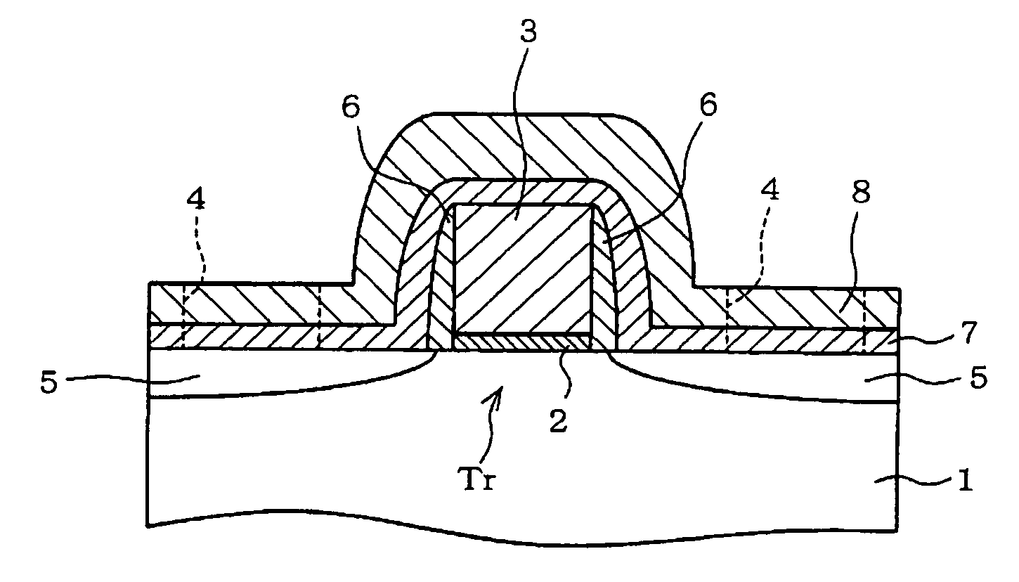
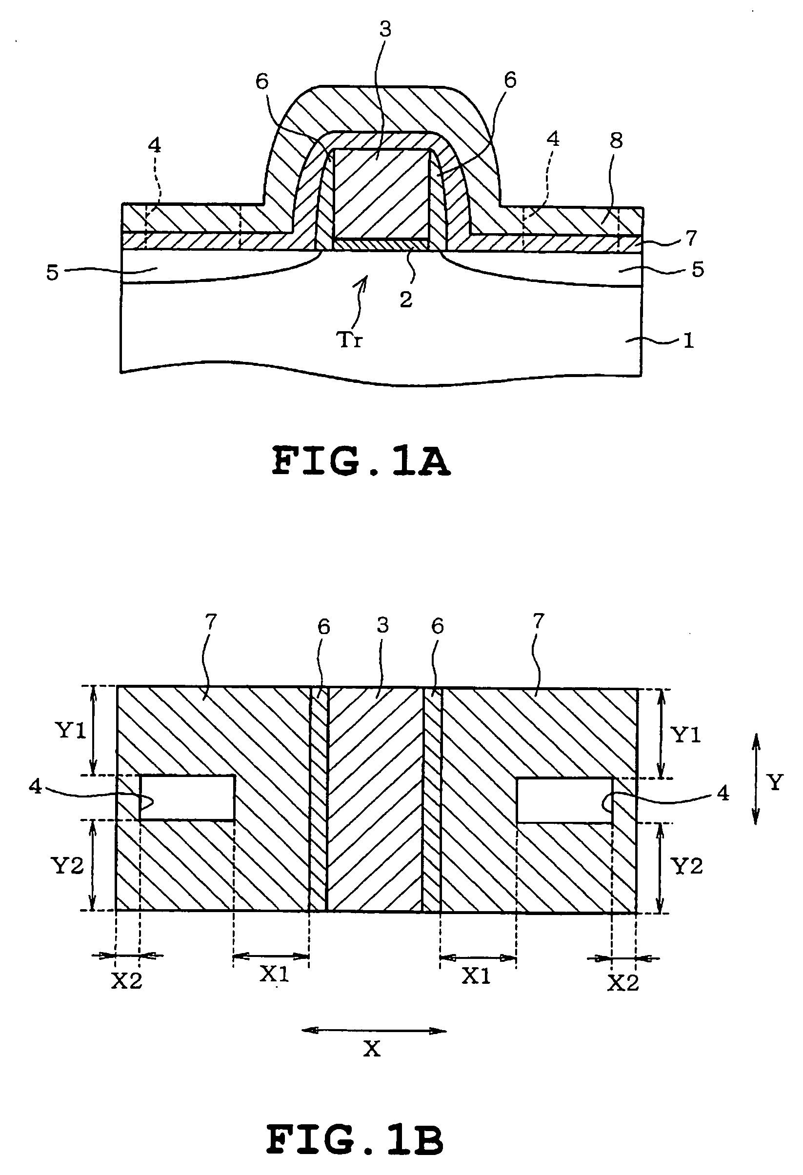
[0038] the semiconductor device in accordance with the present invention will be described with reference to FIGS. 1A to 2. FIGS. 1A and 1B illustrate structures of longitudinal and transverse sections of an n-channel MOS transistor Tr respectively. The n-channel MOS transistor Tr comprises a p-type silicon substrate 1 serving as a semiconductor substrate and a gate insulating film 2 formed on the substrate 1 and a gate electrode 3 further formed on the gate insulating film 2. Two source / drain regions 5 are formed by doping portions of the substrate 1 corresponding to opposite sides of the gate electrode 3 with impurities terminals. The gate insulating film 2 is a silicon oxide film formed by thermal oxidation of a surface of the silicon substrate 1, for example. The gate electrode 3 is formed by depositing metal silicide layers on a polycrystalline silicon layer doped with impurities, for example. The gate electrode 3 has sidewalls on which respective gate sidewall insulating films...
third embodiment
[0059] The invention should not be limited to the foregoing embodiment. The embodiment may be modified or expanded as follows. In the third embodiment, the mobility of the holes as carriers is improved in order that the compressive stress may be applied to the channel region 13. However, the source / drain regions 14 may be made from a material applying tensile stress to the channel region, such as silicon carbide (SiC). In this case, a largest strain can be applied to the surface layer of the channel region 13, whereupon the mobility of the electron serving as a carrier can be improved. This configuration can be applied to the n-channel MOSFET.
[0060] Although the sidewalls of the dummy gate 21 are covered with the silicon nitride films 22 in the third embodiment, another insulating film may be used, instead. Furthermore, a good process can be employed even when no such a film is provided. Additionally, although the silicon substrate 12 is used in the third embodiment, another substra...
fourth embodiment
[0061]FIGS. 8A to 17 illustrate the invention. The invention is applied to an integrated circuit of complementary metaloxide semicondictors (CMOS's). FIGS. 8A to 8D show a semiconductor device comprising, for example, four pairs of CMOS transistors. FIG. 8A is a schematic plan view of the semiconductor device and FIGS. 8B to 8D are sectional views taken along lines 8B-8B, 8C-8C and 8D-8D in FIG. 8A respectively.
[0062] On the silicon substrate 31 are formed four n-channel metal oxide semiconductor field effect transistors (hereinafter “n-MOSFET's”) 32 serving as complementary metal oxide semiconductor (CMOS) transistors and four p-channel MOSFET's (hereinafter “p-MOSFET's”) 33. The n-MOSFET's 32 and p-MOSFET's 33 are arranged in two rows extending in the X direction. Each pair of n-MOSFET 32 and p-MOSFET 33 constituting the CMOS transistor are arranged in the Y direction.
[0063] Each MOS transistor 32 and 33 includes a gate insulating film 34 formed on the silicon substrate 31 and a ...
PUM
 Abstract
Description
Claims
Application Information