High efficiency light emitting device

Inactive Publication Date: 2007-02-08
XEPIX
View PDF6 Cites 64 Cited by
  • Summary
  • Abstract
  • Description
  • Claims
  • Application Information

AI Technical Summary

Benefits of technology

[0012] The present invention relates to III-nitride/II-Oxide optoelectronic devices, and methods of making highly efficient light emitting devices, more particularly to improve performance of III-nitride/II-Oxide light emitting devices.
[0013] In the current approach, as an example, an n++-layer, which can be grown directly on top of the p-Ga(Al, In)N layer in normal LED structures using the MOCVD or similar epitaxial growth technique, is adopted to form a tunneling junction with the p-Ga(Al, In)N layer. The n++-layer can be made of GaN, InGaN, AlGaN, AlInGaN, or short period superlattice (SPS) layers consisting of any two of these materials, such as InGaN/GaN SPS. After that, a layer of n+-GaN can be grown or attached on top of the tunneling layer. By optimizing the growth conditions with higher doping concentration, the top n+-layer can be made highly conductive and show very rough surface. Therefore, it can serve dual functions. One is to act as a current spreading layer to improve the hole injection uniformity and efficiency. Another function is to increase light extraction due to the rough surface.
[0014] The top n+-GaN layer has an absorption band at shorter wavelengths than for the p-Ga(Al

Problems solved by technology

However, the difficulty in ionizing Mg dopants inevitably results in a highly resistive p-Ga(Al, In)N layer, large metal/p-Ga(Al, In)N contact resistance, and poor current spreading.
These drawbacks limit the performance of the III-nitride-based LEDs.
In addition, the optical transmittance of the p-metal layer is an important issue to be taken into account since photons generated in the active region tend to be partially absorbed by this layer.
Increasing the doping level of Mg for higher conductivity is not effective, and would increase the light absorption substantially.
However, Ni—Au layer partially absorbs photons generated in the active region, which lowers the LED light output.
This prior art LED 200 shown in FIG. 2, however, requires post-deposition of the ITO layer after epitaxial growth of the LED structure, and more complicated processing procedure to roughen the ITO layer for light extraction enhancement as described by K. M. Chang, J. Y. Chu, C. C

Method used


Image

  • High efficiency light emitting device
  • High efficiency light emitting device
  • High efficiency light emitting device

Examples


Embodiment Construction

[0035] In the following description of the preferred implementation, reference is made to the accompanying drawings that form a part hereof, and in which is shown by way of illustration a specific implementation in which the invention may be practiced. It is to be understood that other implementations may be utilized and structural changes may be made without departing from the scope of the present invention.

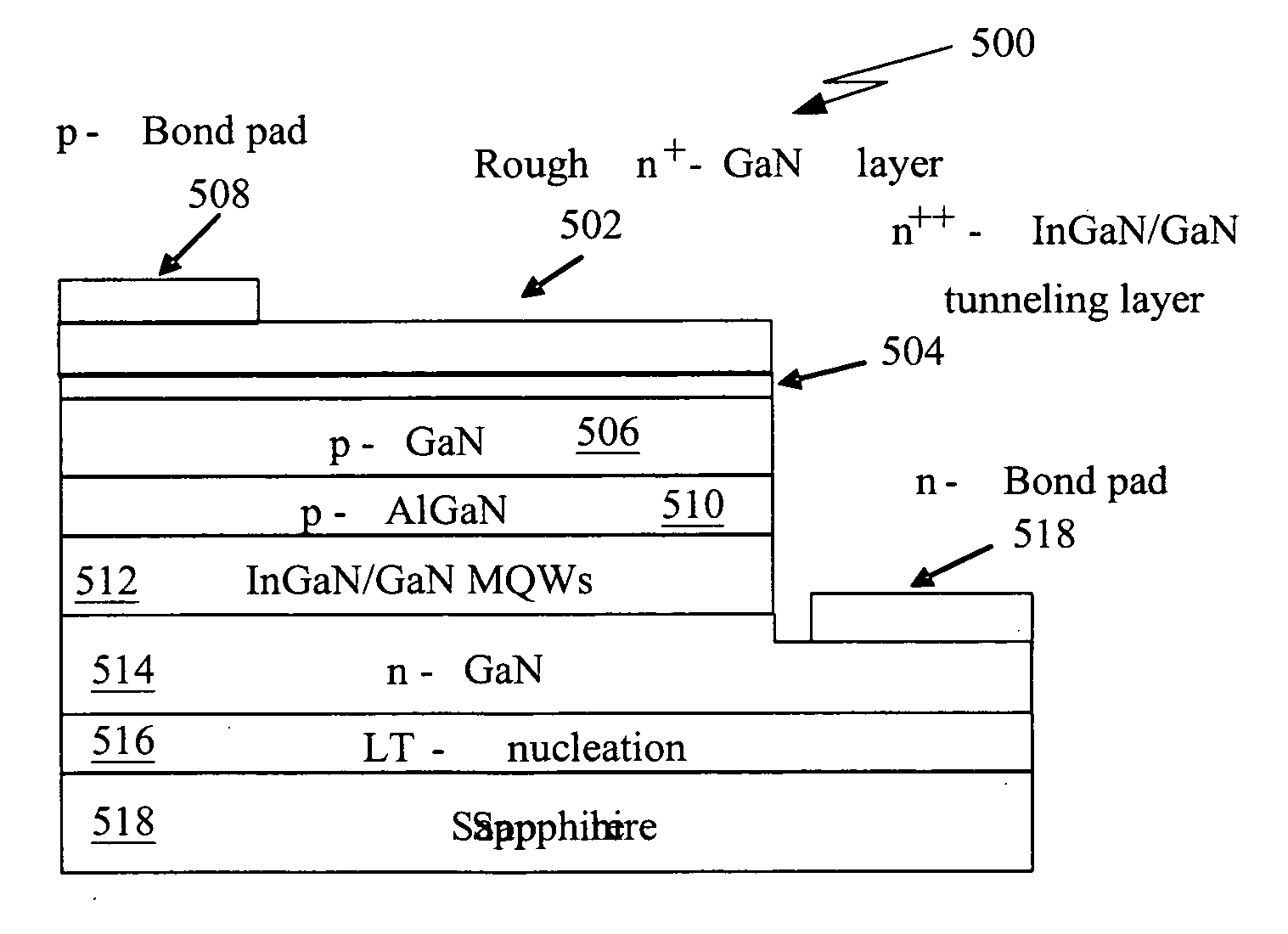
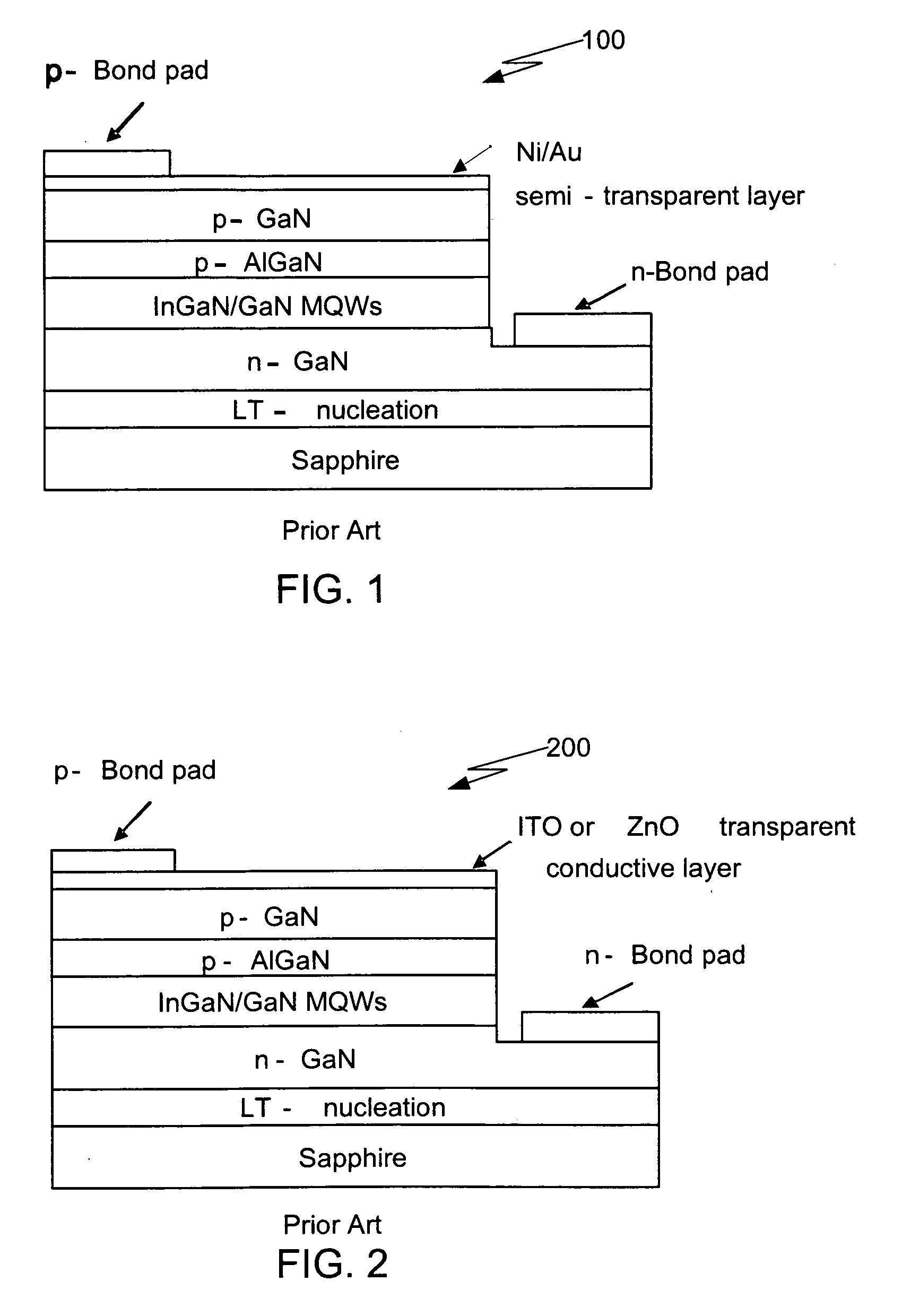
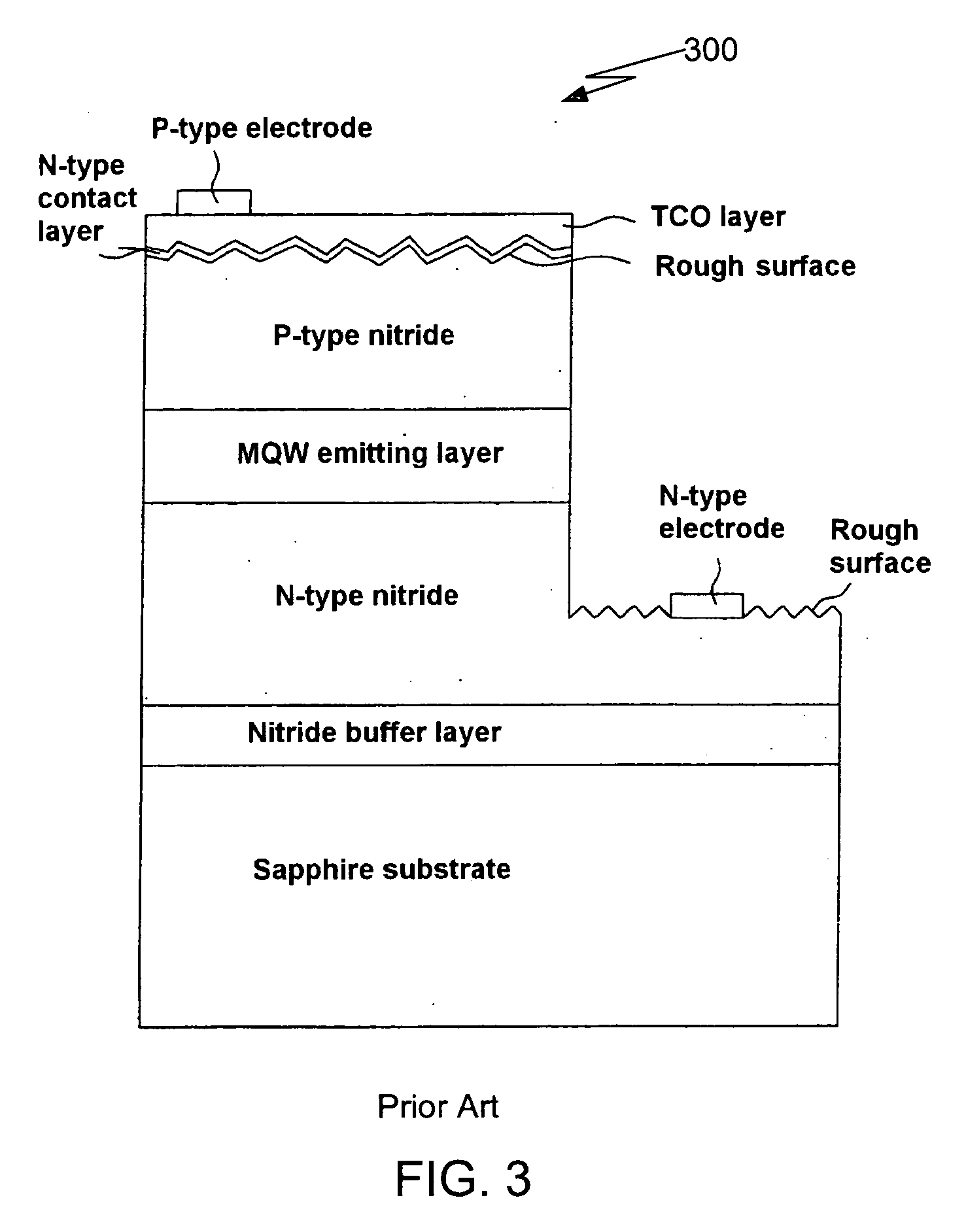
[0036] The present implementation reveals a high efficiency III-Nitride LED. Compared with the conventional LED, an additional n+-GaN layer and an n++-tunneling layer directly grown on top of the p-Ga(Al, In)N surface are utilized to improve both current spreading and light extraction of a high efficiency III-Nitride LED. This high efficiency III-Nitride LED has demonstrated significant improvement in light output, 70% more than conventional LEDs, or 30% more than the prior-art LEDs. The manufacture of the high efficiency III-Nitride LED is by a simplified process as compared t...


PUM


Abstract

A highly efficient III-nitride/II-Oxide light emitting device that has a n++-tunneling layer, which comprises at least one material selected from a group consisting of n++-GaN, n++-InGaN, n++-AlGaN, n++-AlGaInN, n++-ZnO, n++-ZnCdO, n++-ZnMgO, n++-ZnMgCdO, that is deposited on top of the p-layer in a LED structure. After that, a top n-layer is deposited above that n++-tunneling layer that may be a n+-layer and comprises at least one material selected from a group consisting of n+-GaN, n+-InGaN, n+-AlGaN, n+-AlGaInN, n+-ZnO, n+-ZnCdO, n+-ZnMgO, n+-ZnMgCdO or a top n-layer may also be a n++-layer and comprises at least one material selected from a group consisting of n++-GaN, n++-InGaN, n++-AlGaN, n++-AlGaInN, n++-ZnO, n++-ZnCdO, n++-ZnMgO, n++-ZnMgCdO so that the top n-layer is made highly conductive and show very rough surface.

Description

BACKGROUND OF THE INVENTION [0001] 1. Field of the Invention [0002] The invention relates to high efficiency light emitting devices, and more particularly to III-nitride / II-Oxide light emitting devices. [0003] 2. Related Art [0004] There is a growing demand worldwide for solid state visible and ultraviolet (UV) light emitting diodes (LEDs) due to their huge, expanding market for applications such as traffic lights, full color displays, LCD back-lighting, automobile, stage, and museum lighting, and general illumination. Typically, most commercial solid state LEDs are III-nitride based LEDs, which use Mg-doped III-nitride layers as the top p-type contact material. However, the difficulty in ionizing Mg dopants inevitably results in a highly resistive p-Ga(Al, In)N layer, large metal / p-Ga(Al, In)N contact resistance, and poor current spreading. These drawbacks limit the performance of the III-nitride-based LEDs. Therefore, what is needed in the art is an approach that reduces the conta...

Claims


Application Information

Patent Timeline
IPC IPC(8): H01L31/109
CPCH01L33/007H01L33/04H01L33/44H01L33/32H01L33/22
Inventor XIN, HUOPINGLIU, XINGQUANSHI, XIAOHONGCHOI, CHAN KYUNGSONG, JIN SOO
Owner XEPIX
Why Eureka
Try Eureka