Dielectric film and process for its fabrication

a technology of dielectric film and fabrication process, which is applied in the direction of electrically conductive connections, chemical coatings, coatings, etc., can solve the problems of not being able to obtain dielectric films with satisfactory levels, and the dielectric constant of the obtained dielectric films is not sufficiently high, so as to prevent the vaporization of metal during baking, high dielectric constant, and excellent leakage characteristics

Active Publication Date: 2007-03-01
TDK CORPARATION
View PDF12 Cites 14 Cited by
  • Summary
  • Abstract
  • Description
  • Claims
  • Application Information

AI Technical Summary

Benefits of technology

[0012] More preferably, the metal layer is Cu, and at least part of the baking step involves heating of the precursor layer in a reduced pressure atmosphere prepared to a pressure of between 0.01 Pa and 100 Pa. In another preferred mode, the metal layer is Ni, and at least part of the baking step involves heating of the precursor layer in a reduced pressure atmosphere prepared to a pressure of between 0...

Problems solved by technology

Yet although it has been possible to prevent oxidation of metals such as Cu during baking with the conventional art methods, the obtained dielectric films have n...

Method used


Image

  • Dielectric film and process for its fabrication
  • Dielectric film and process for its fabrication
  • Dielectric film and process for its fabrication

Examples


example 1

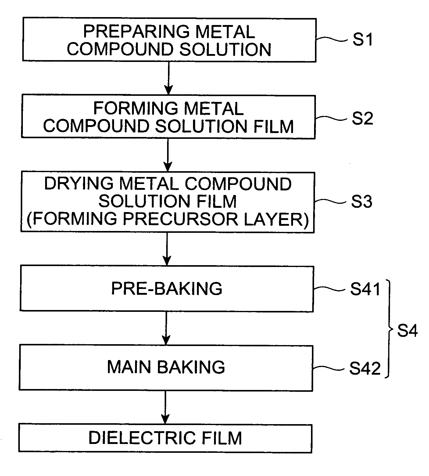
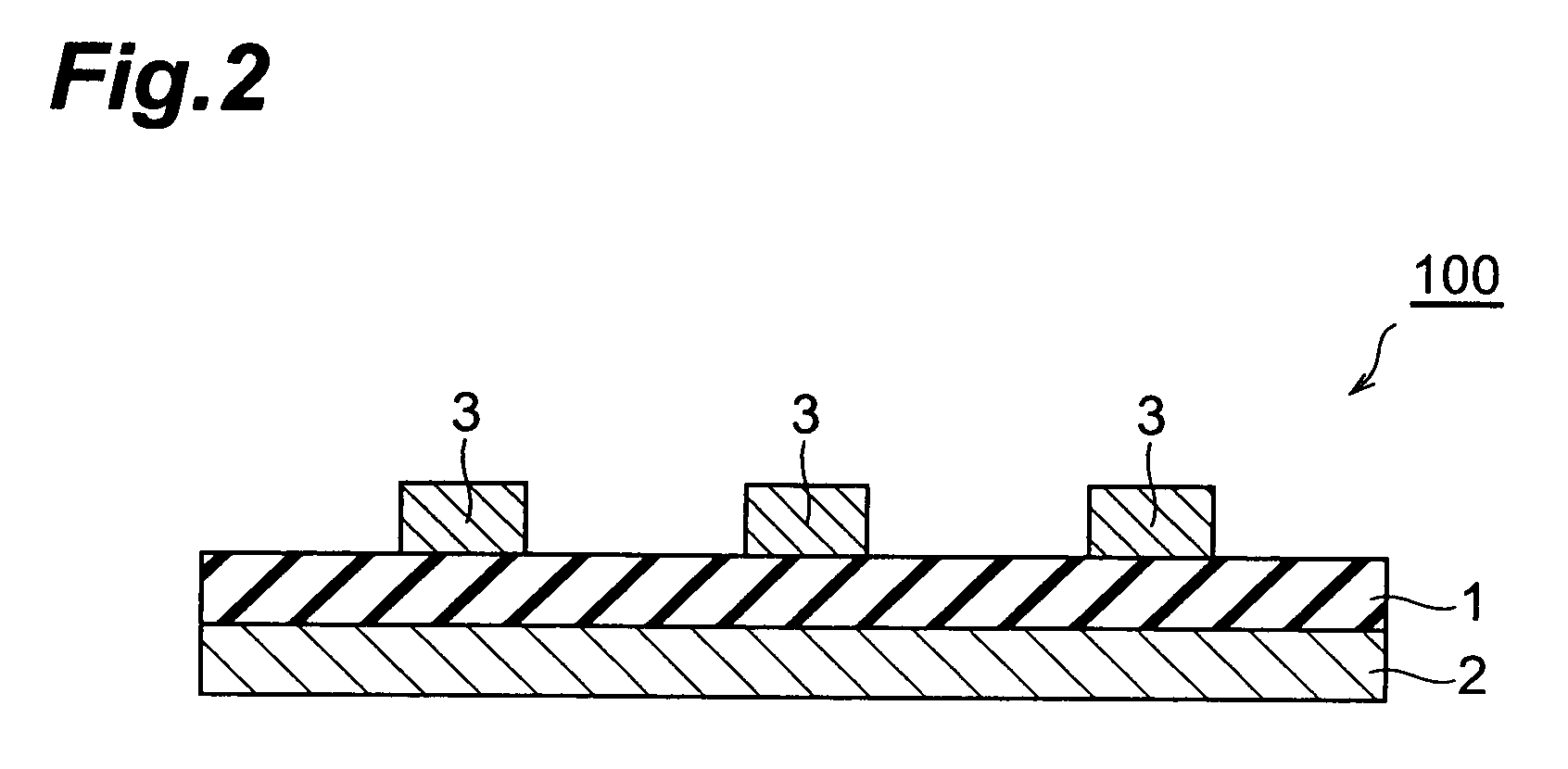
[0034] Metal alkoxides containing Ba, Sr and Ti were mixed with isoamyl acetate and amyl alcohol in a weight ratio of 20:70:10 and dissolved to obtain a precursor solution, which was applied onto a copper foil (product of Nilaco, 100 μm thickness, rolled foil) as the lower electrode by spin coating (3000 rpm, 15 sec). After application, it was heated in air on a hot plate at 150° C. for 10 minutes to dry the film and form a precursor layer on the copper foil.

[0035] Next, the laminate comprising the copper foil and precursor layer was placed in an infrared heating furnace and a reduced pressure atmosphere was formed in the furnace using a vacuum pump to a pressure of 0.1 Pa as measured by a manometer at room temperature. The temperature in the furnace was raised to 400° C. while continuing pressure reduction with the vacuum pump, for 30 minutes of heating in that condition (pre-baking). The same application, drying and pre-baking were repeated 4 to 6 times to obtain a precursor laye...

example 2

[0037] A precursor solution containing 2-ethylhexanoic acid salts of Ba, Sr and Ti as metal oxide precursors was applied onto a Ni foil (product of Nilaco, 100 μm thickness, rolled foil) as the lower electrode by spin coating (3000 rpm, 20 sec). After application, it was heated in air on a hot plate at 150° C. for 10 minutes to dry the film and form a precursor layer on the nickel foil. Next, the precursor layer was heated at 400° C. for 10 minutes on a hot plate in air (pre-baking). The same application, drying and pre-baking were repeated 10 times to obtain a precursor layer with the prescribed thickness. This was followed by further heating for 30 minutes at 800° C. in an infrared heating furnace with the pressure reduced to 0.05 Pa by the same method as in Example 1, to form a dielectric film (main baking). Next, a Pt electrode was formed on the dielectric film by sputtering, as the upper electrode. The dielectric property and leak current of the fabricated dielectric film were ...


PUM

PropertyMeasurementUnit
Temperatureaaaaaaaaaa
Pressureaaaaaaaaaa

Abstract

A dielectric film production process comprising a baking step in which a dielectric film is formed by heating a precursor layer formed on a metal layer, wherein the metal layer contains at least one type of metal selected from the group consisting of Cu, Ni, Al, stainless steel and inconel, and during at least part of the baking step the precursor layer is heated in a reduced pressure atmosphere.

Description

BACKGROUND OF THE INVENTION [0001] 1. Field of the Invention [0002] The present invention relates to a dielectric film and to a process for its fabrication. [0003] 2. Related Background Art [0004] Solution methods are known as methods for forming dielectric films containing metal oxides such as barium strontium titanate (BST) on metal layers. In such solution methods, a solution containing prescribed starting materials is coated onto a metal layer and dried, and the formed precursor layer is baked to form a dielectric film. However, when the metal composing the metal layer is a readily oxidizing metal such as Cu or Ni, the metal layer becomes oxidized during the baking, thereby losing conductivity. When oxidation of the metal occurs, even if the dielectric constant of the dielectric layer itself is increased, for example, the capacity of the capacitor does not adequately increase. In order to prevent oxidation of the metal layer, therefore, there have been proposed methods such as a...

Claims


Application Information

Patent Timeline
IPC IPC(8): H01L21/44H01L21/31
CPCC23C18/1216C23C18/1241H01L21/31691C23C18/1283C23C18/125H01L21/02263H01L21/31
Inventor MIYAMOTO, YUKISAITA, HITOSHI
Owner TDK CORPARATION
Why Eureka
Try Eureka