Apparatus and method for inspecting a sample of a specimen by means of an electron beam

Active Publication Date: 2007-03-15
ICT INTEGRATED CIRCUIT TESTING GESELLSCHAFT FUER HALBLEITERPRUEFTECHNIK GMBH
View PDF12 Cites 32 Cited by
  • Summary
  • Abstract
  • Description
  • Claims
  • Application Information

AI Technical Summary

Benefits of technology

[0022] With the method, it is possible to locate a defect on a wafer (SEM mode), to fabricate a membrane from the wafer (FIB mode) and inspect the membrane by means of transmitted electrons (transmission mode) with only one electron beam device and only one ion beam device. This way, a surface image and a complementary cross sectional image of a defective region of a integrated circuit can be obtained in a

Problems solved by technology

However, depending on the electron beam spot size and the thickness of the sample, a spatia

Method used


Image

  • Apparatus and method for inspecting a sample of a specimen by means of an electron beam
  • Apparatus and method for inspecting a sample of a specimen by means of an electron beam
  • Apparatus and method for inspecting a sample of a specimen by means of an electron beam

Examples


Example

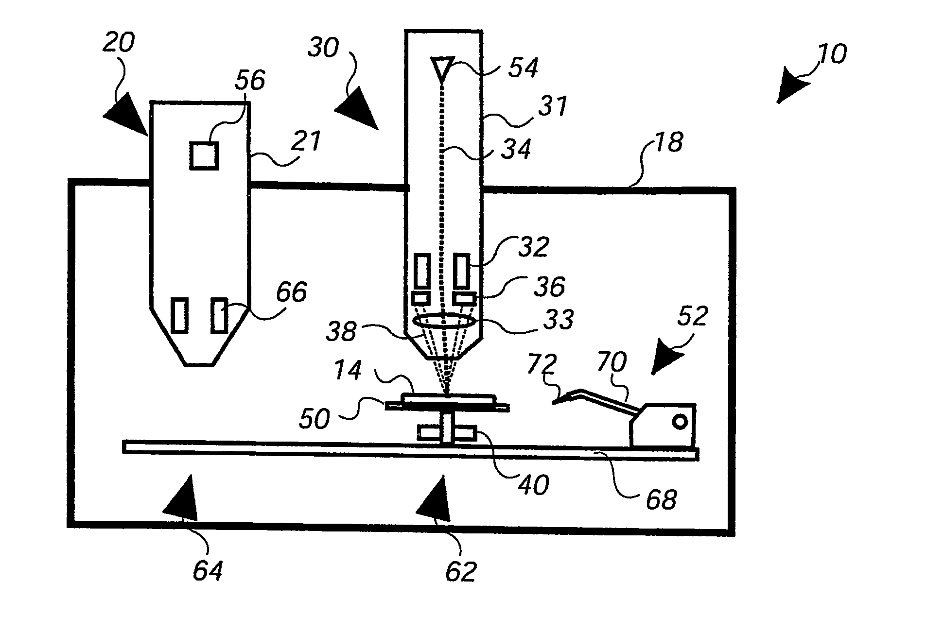
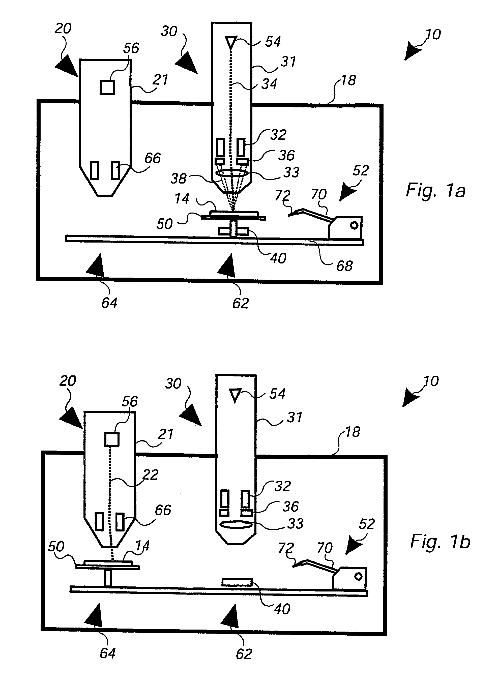
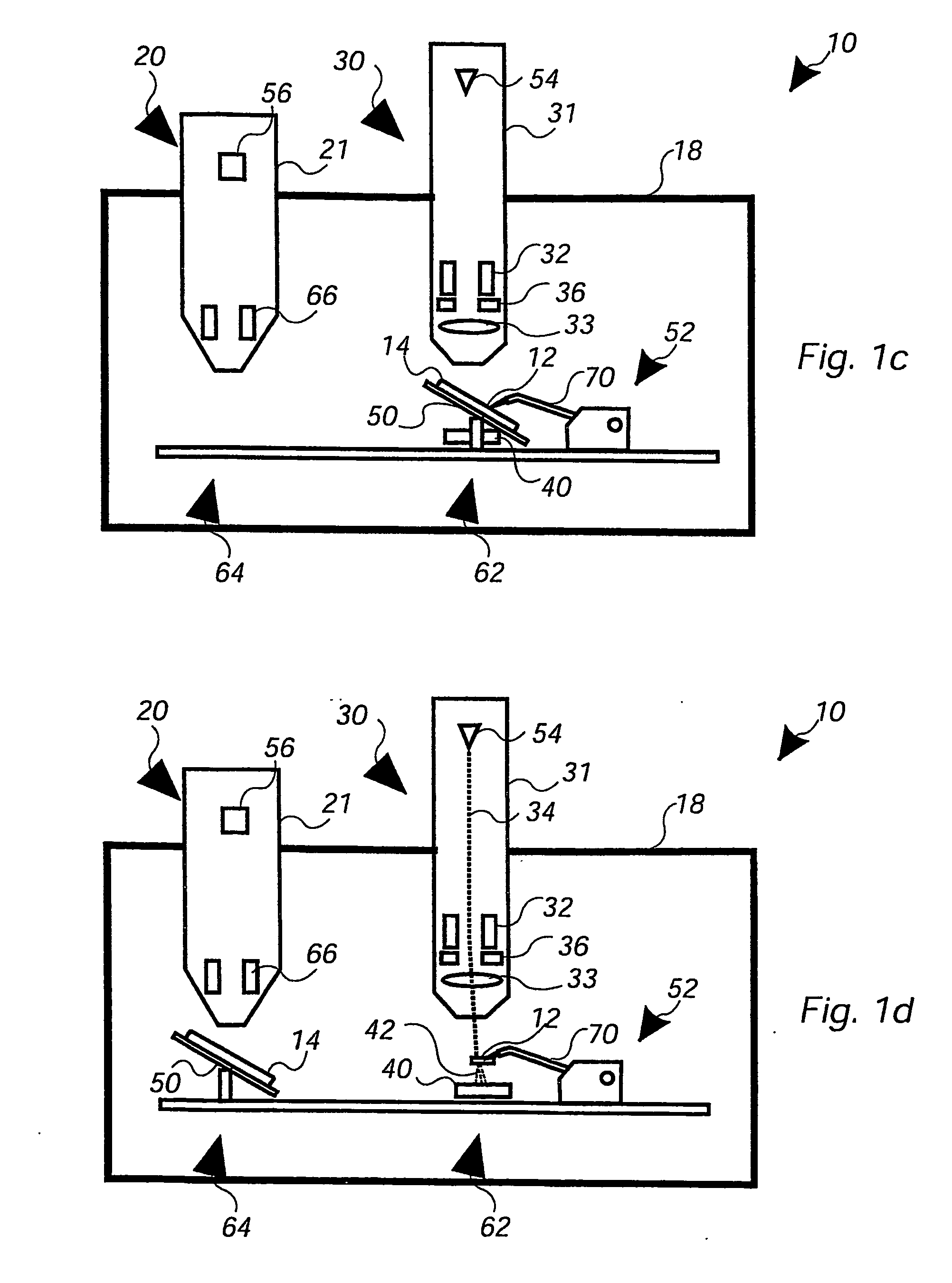
[0027] In the description of the detailed embodiments below, the numbers refer to the enclosed FIGS. 1a to 1d, 2 and 3. However, the figures only represent particular, non-limiting embodiments of the invention which only have the purpose of being illustrative examples. The description below, even though it makes reference to the figures, is to be understood in a broad sense and includes any deviation from the described embodiments which is obvious to a person skilled in the art.

[0028] Generally, the apparatus 10 according to the invention is meant to be used for the inspection of any sample 12 of a specimen 14 which is suitable for transmission microscopy inspection. Preferably, the specimen 14 is a solid substrate like, e.g., a semiconductor wafer or chip, and, preferably, the sample 12 thereof is a cross sectional thin slice of the wafer or chip. For such an inspection, the inspection of the wafer 14 with the electron beam device 30 using the first detector 36 results in an image...


PUM


Abstract

The invention refers to an apparatus (10) for inspecting a sample (12) of a specimen (14) by means of an electron beam (34) comprising a vacuum chamber (18); an ion beam device (20) for generating an ion beam (22) used for etching a sample (12) from the specimen (14) within said vacuum chamber (18); an electron beam device (30) having a scanning unit (32) for scanning the electron beam (34) across said specimen (14) within said vacuum chamber (18); said electron beam device (30) having a first detector (36) positioned to detect electrons (38) that are released from the specimen (14) in a backward direction with respect to the direction of the electron beam (34); and said electron beam device (30) having a second detector (40) positioned to detect electrons (42) that are released from the sample (12) of the specimen (14) in a forward direction with respect to the direction of the electron beam (34); and separation means (50; 52) within said vacuum chamber (18) to separate the sample (12) from the specimen (14) for the inspection of the sample (12) by means of the second detector (40). With the apparatus according to the invention, it is possible to perform a transmission inspection of a sample of a specimen, e.g. a thin slice of a semiconductor wafer, at a high throughput at comparably low costs.

Description

FIELD OF THE INVENTION [0001] The invention relates to an apparatus and method for inspecting a sample of a specimen by means of an electron beam. In particular, the invention relates to an apparatus and method for inspecting a thin slice of a semiconductor wafer. BACKGROUND OF THE INVENTION [0002] For progress in microelectronics, it is important to have tools for inspecting microelectronical structures on a chip or wafer with ever increasing spatial resolution. At the same time, it is important to decrease the costs of such inspections in order for the industry to fabricate devices of ever increasing complexity at low costs. [0003] A prominent tool for such inspections is the scanning electron microscope (SEM). The SEM uses a primary electron beam as a means to probe the surface structure of a given specimen. An interaction of the primary electron beam with the specimen causes electrons to be released into a backward direction with respect to the primary electron beam where they a...

Claims


Application Information

Patent Timeline
IPC IPC(8): G21K7/00G01N1/32H01J37/28H01J37/305
CPCG01N1/32H01J37/28H01J2237/31745H01J2237/20H01J37/3056
Inventor FEUERBAUM, HANS-PETER
Owner ICT INTEGRATED CIRCUIT TESTING GESELLSCHAFT FUER HALBLEITERPRUEFTECHNIK GMBH
Why Eureka
Try Eureka