

Methods of preparing a multi-shell nanocrystal structure, multi-shell nanocrystal structures and fabricated device including the same
a nanocrystal and nanocrystal technology, applied in the field of forming a multi-shell nanocrystal structure, multi-shell nanocrystal structure and a method for fabricating a device, can solve problems such as the decrease of quantum efficiency, and achieve the effect of increasing the luminescence efficiency and high luminescence efficiency of the multi-shell nanocrystal structur
- Summary
- Abstract
- Description
- Claims
- Application Information
AI Technical Summary
Benefits of technology
Problems solved by technology
Method used
Image

Examples
example 1
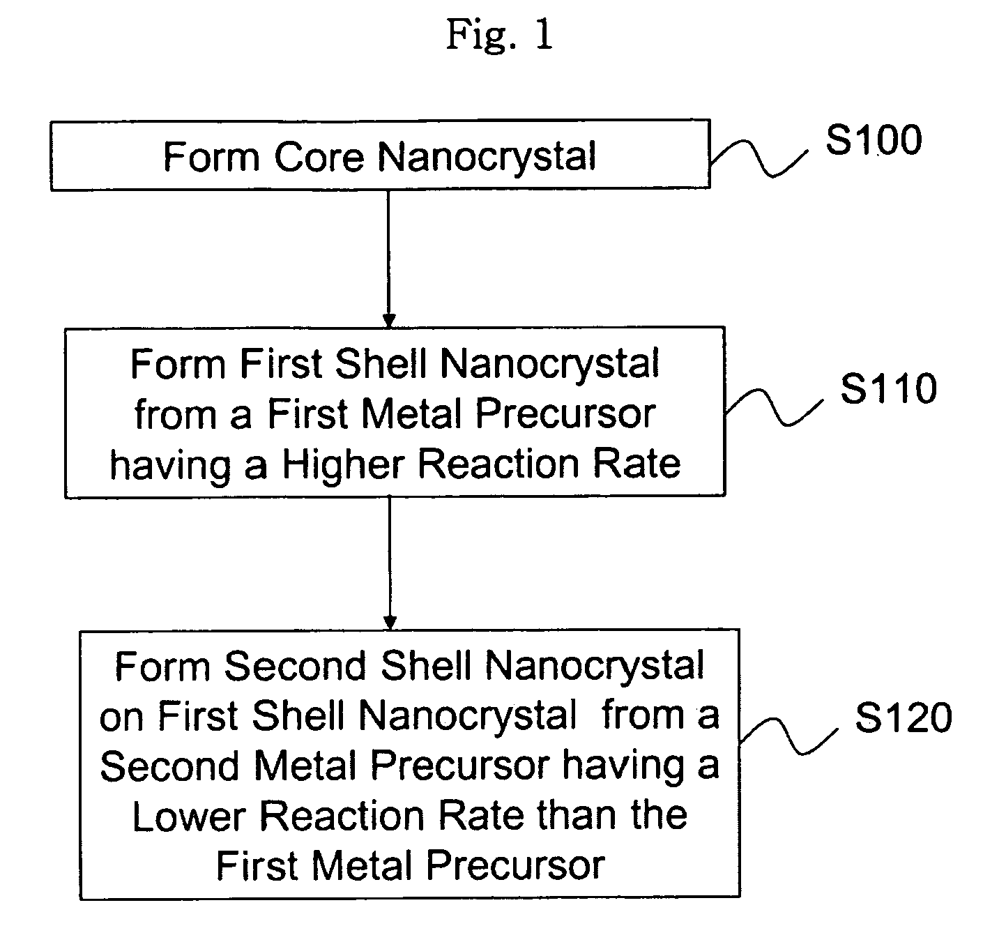
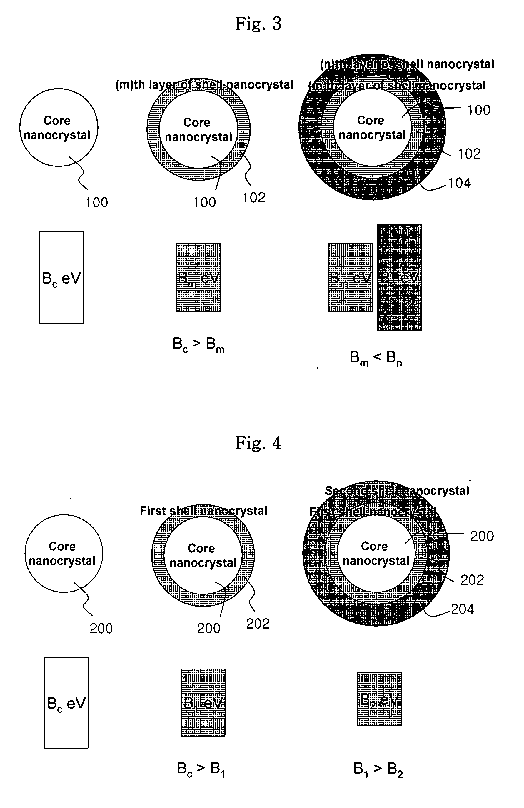
Formation of CdSe / CdS.ZnS Nanocrystals According to Changes in Ratio between Metal Precursors
[0096] About 16 g of trioctylanine (TOA), about 2 g of oleic acid and about 1.6 mmol of cadmium oxide were simultaneously placed in a 125-ml flask equipped with a reflux condenser. The reaction temperature of the mixture was adjusted to about 300° C. with stirring.
[0097] Selenium (Se) powder was dissolved in trioctylphosphine (TOP) to obtain a Se—TOP complex solution with a Se concentration of about 0.2M. About 2 ml of the Se—TOP complex solution were added to the previous reaction mixture. The reaction continued to stir for about 30 seconds.
[0098] After completion of the reaction, the reaction mixture was cooled to about room temperature as rapidly as possible. Ethanol, a non-reactive solvent, was added to the reaction mixture, and then the resulting mixture was centrifuged. The precipitate obtained from centrifugation was separated from the supernatant, and dispersed in toluene to prepa...
example 2
Formation of CdSe / CdS.ZnS Nanocrystals According to Changes in Size of CdSe Core Nanocrystal
[0103] About 16 g of TOA, about 2 g of oleic acid and about 1.6 mmol of cadmium oxide were simultaneously placed in a 125-ml flask equipped with a reflux condenser. The reaction temperature of the mixture was adjusted to about 300° C. while continuing to stir. Separately, selenium (Se) powder was dissolved in trioctylphosphine (TOP) to obtain a Se—TOP complex solution with a Se concentration of about 0.2M. About 2 ml of the Se—TOP complex solution were added to the previous reaction mixture. The reaction was allowed to proceed for about 30 seconds to prepare a CdSe nanocrystal that emits light at a wavelength of about 586 nm.
[0104] About 16 g of TOA, about 0.3 g of octadecyl phosphonic acid and about 0.4 mmol of cadmium oxide were simultaneously placed in a 125-ml flask equipped with a reflux condenser. While stirring, the reaction temperature of the mixture was adjusted to about 300° C. Se...
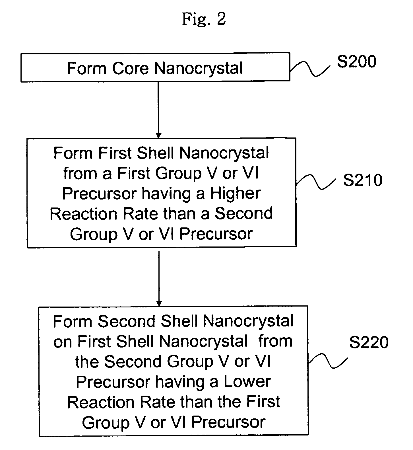
example 3
Formation of CdSe / ZnSe.ZnS Nanocrystals
[0112] 16 g of trioctylamine (TOA), about 0.3 g of octadecyl phophonic acid and about 0.4 mmol of cadmium oxide were simultaneously placed in a 125-ml flask equipped with a reflux condenser. The reaction temperature of the mixture was adjusted to about 300° C. while continuing to stir. A selenium (Se) powder was dissolved in trioctylphosphine (TOP) to obtain an Se—TOP complex solution with a Se concentration of about 2M. About 2 ml of the Se—TOP complex solution were added to the previous reaction mixture. The reaction was allowed to proceed for about 2 minutes to prepare a CdSe nanocrystal that emits light at a wavelength of about 486 nm.
[0113] After completion of the reaction, the reaction mixture was cooled to about room temperature as rapidly as possible. Ethanol, a non-reactive solvent, was added to the reaction mixture, and then the resulting mixture was centrifuged. The precipitate obtained from centrifugation was separated from the su...
PUM
| Property | Measurement | Unit |
|---|---|---|
| Temperature | aaaaa | aaaaa |
| Temperature | aaaaa | aaaaa |
| Time | aaaaa | aaaaa |
Abstract
Description
Claims
Application Information