Group III nitride semiconductor stacked structure and production method thereof

a technology of stacked structure and nitride, which is applied in the direction of semiconductor/solid-state device manufacturing, semiconductor devices, electrical devices, etc., can solve the problems of difficult growth of single crystals, inability to obtain satisfactory crystallinity, and difficulty in growing single crystals, etc., to achieve high-efficiency light-emitting devices and low cost

Active Publication Date: 2007-04-12
TOYODA GOSEI CO LTD
View PDF16 Cites 43 Cited by
  • Summary
  • Abstract
  • Description
  • Claims
  • Application Information

AI Technical Summary

Benefits of technology

[0016] An object of the present invention is to provide a group III nitride semiconductor stacked structure having a high-quality A-plane group III nitride semiconductor layer on an R-plane sapphire substrate. In addition, an object of the present invention is to provide a simple production method for a group III nitride semiconductor stacked structure having a high-quality A-plane group III nitride semiconductor layer on an R-plane sapphire substrate.
[0034] According to the present invention, a high-quality yet inexpensive A-plane group III nitride semiconductor layer can be stacked onto an R-plane sapphire substrate using a simple method consisting of controlling the growth temperature of a group III nitride semiconductor. In addition, despite the resulting group III nitride semiconductor stacked structure having a thin group III nitride semiconductor layer of 20 μm or less, it is extremely flat, the surface is extremely flat, it has a pit density of 1×1010 cm−2 or less, and it is extremely useful as a material of an inexpensive and highly efficient light-emitting device.

Problems solved by technology

As group III nitride semiconductors have a dissociation pressure which reaches 2,000 atmospheres at the growth temperature of single crystals, it is difficult to grow single crystals, and the use of single crystals of group III nitride semiconductors as substrates used for epitaxial growth in the manner of other group III-V compound semiconductors is difficult under the present circumstances.
In general, in the case of the existence of a high degree of lattice mismatch such as this, it is difficult to grow crystals directly on a substrate by epitaxial growth and, even if the crystals are grown, crystals with satisfactory crystallinity are not obtained.
Deterioration of device characteristics occurs resulting in problems in devices, such as light-emitting devices, due to this type of piezoelectric field.
Factors behind the low external quantum efficiency of green LEDs consist of not only poor crystallinity of the emission layer GaInN (crystal deterioration caused by increased In composition), but also the afore-mentioned effects produced by piezoelectric fields due to the use of longer wavelengths.
On the other hand, as routinely used C-plane sapphire substrate is the most difficult type of sapphire substrate to produce while also being expensive, LEDs produced on this substrate are expensive.
However, group III nitride semiconductors produced on R-plane sapphire substrates are susceptible to the formation of pits in the surface, and it has been difficult to produce a high-quality group III nitride semiconductor layer on an R-plane sapphire substrate.
In the case of epitaxial lateral overgrowth, the process is complex due to the need to form a mask pattern and to repeat the growth several times by re-growing.
In addition, a thick film group III nitride semiconductor layer is required, thereby increasing costs.

Method used


Image

  • Group III nitride semiconductor stacked structure and production method thereof
  • Group III nitride semiconductor stacked structure and production method thereof
  • Group III nitride semiconductor stacked structure and production method thereof

Examples


example 1

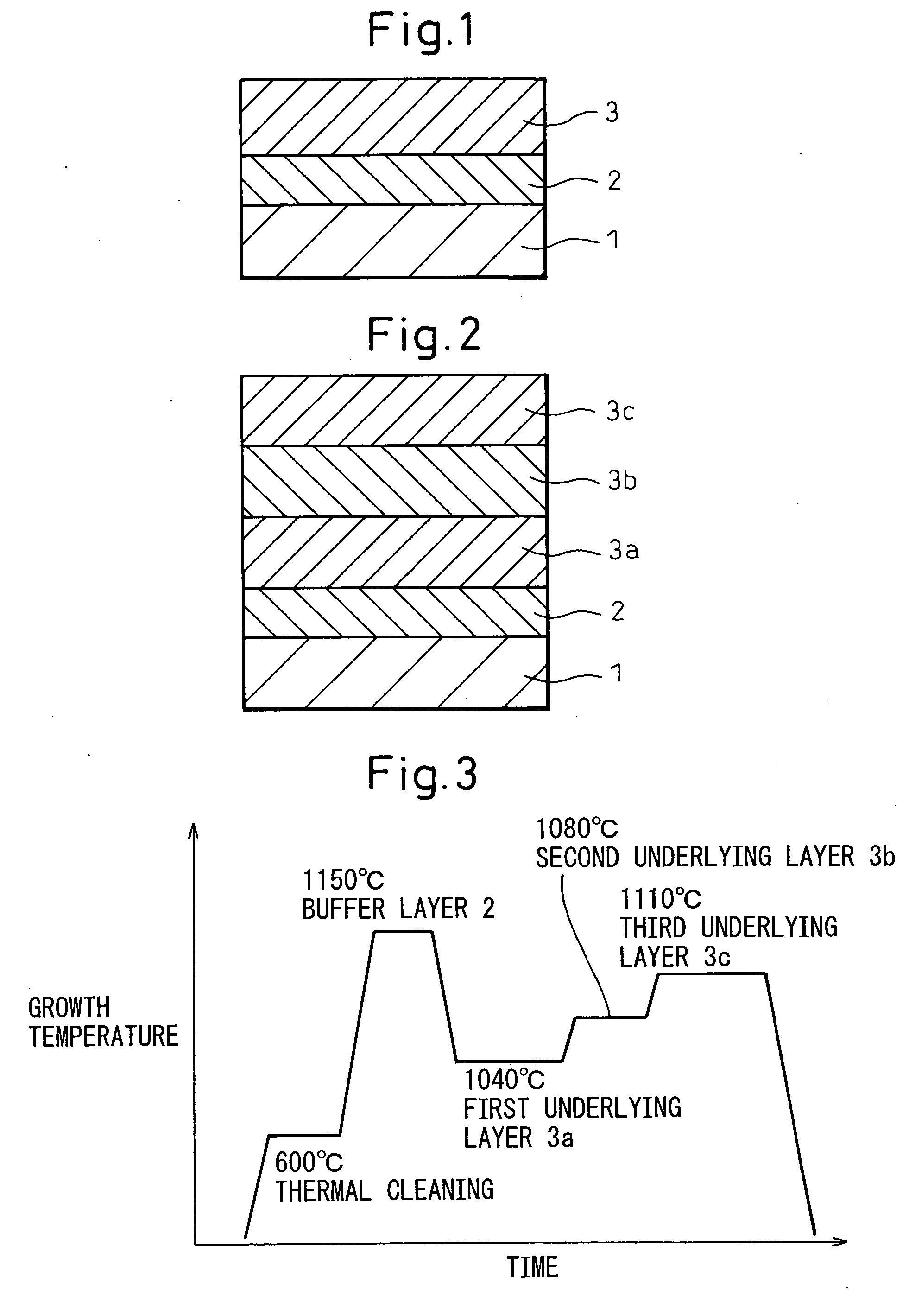
[0075]FIG. 2 is a schematic drawing showing a cross-section of a group III nitride semiconductor stacked structure produced in the present example, while FIG. 3 is a graph showing the temperature profile of each step in the present example. The aforementioned structure was formed in the order indicated below using a typical reduced-pressure MOCVD. First, an R-plane sapphire substrate 1 was placed on a high-purity graphite semiconductor susceptor heated to a growth temperature with a radio-frequency (RF) induction heater. After placing the substrate on the susceptor, nitrogen gas was introduced into a stainless steel vapor phase growth reactor to purge the inside of the reactor.

[0076] After circulating nitrogen gas through the vapor phase growth reactor for 8 minutes, the induction heater was activated to raise the temperature of the substrate 1 from room temperature to 600° C. over a period of 10 minutes. Hydrogen gas and nitrogen gas were then circulated through while maintaining ...

example 2

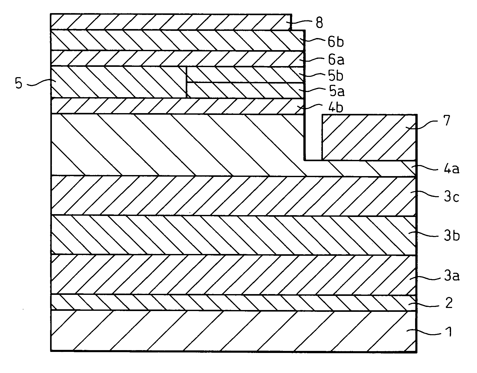
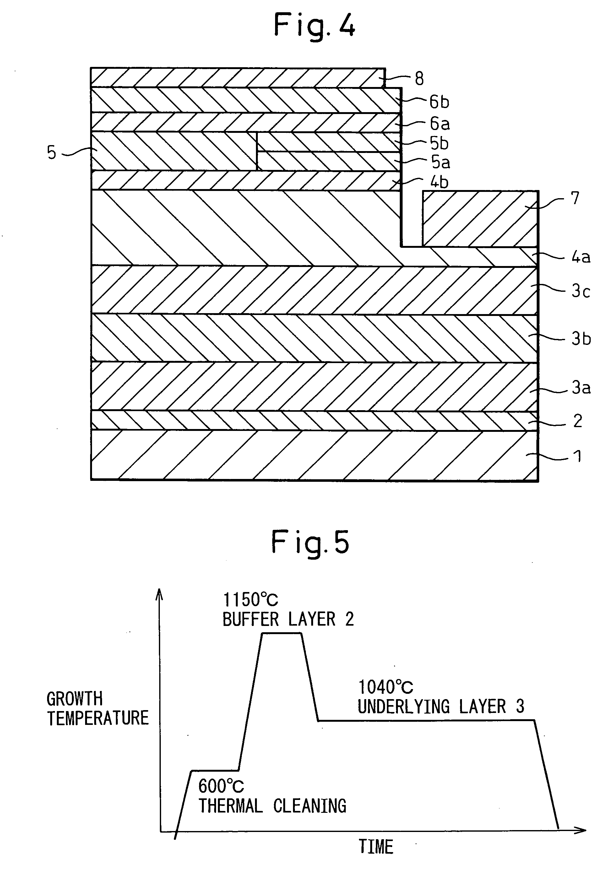
[0086] A group III nitride semiconductor layer was additionally stacked onto the stacked structure produced in Example 1 to produce a group III nitride semiconductor light-emitting device. FIG. 4 is a drawing schematically showing the cross-sectional structure of the group III nitride semiconductor light-emitting device produced in this example.

[0087] After producing the device through the third underlying layer 3c by repeating the procedure described in Example 1, an n-type contact layer 4a composed of Si-doped n-type GaN was formed. After stacking the n-type contact layer 4a, an n-type clad layer 4b composed of Si-doped n-type In0.03Ga0.97N was stacked at 730° C. This n-type clad layer 4b was grown to a layer thickness of 12.5 nm using triethyl gallium (TEG) for the gallium source and trimethyl indium (TMI) for the indium source.

[0088] Next, a multi-quantum well structure light-emitting layer 5 having a pentacyclic structure, composed of a barrier layer 5a composed of GaN and a ...


PUM

PropertyMeasurementUnit
thicknessaaaaaaaaaa
temperatureaaaaaaaaaa

Abstract

An object of the present invention is to provide a group III nitride semiconductor stacked structure having a high-quality A-plane group III nitride semiconductor layer on an R-plane sapphire substrate. The inventive group III nitride semiconductor stacked structure comprises a substrate composed of R-plane sapphire (α-Al2O3), a buffer layer composed of aluminum gallium nitride (AlxGa1−xN: 0≦X≦1) formed on said substrate and an underlying layer composed of an A-plane group III nitride semiconductor (AlxGayInzN1−aMa: 0≦X≦1, 0≦Y≦1, 0≦Z≦1, and X+Y+Z=1; wherein, M represents a group V element other than nitrogen (N), and 0≦a≦1) formed on said buffer layer, wherein the pit density of the surface of said underlying layer is 1×1010 cm−2 or less.

Description

CROSS REFERENCE TO RELATED APPLICATION [0001] This application is an application filed under 35 U.S.C. §111(a) claiming benefit, pursuant to 35 U.S.C. §119(e)(1), of the filing date of the Provisional Application No. 60 / 726,526 filed on Oct. 14, 2005, pursuant to 35 U.S.C. §111(b).TECHNICAL FIELD [0002] The present invention relates to a group III nitride semiconductor stacked structure, to a production method thereof, more particularly, to a group III nitride semiconductor stacked structure having a high-quality A-plane group III nitride semiconductor layer on an inexpensive R-plane sapphire substrate, and to a production method thereof. BACKGROUND ART [0003] As group III nitride semiconductors have a direct energy transition band gap equivalent to the region from visible light to ultraviolet light, enabling highly efficient emission of light, they have been commercialized as light-emitting diodes (LEDs) and laser diodes (LDs). In addition, they also have a potential for use as ele...

Claims


Application Information

Patent Timeline
Patent Type & Authority Applications(United States)
IPC IPC(8): H01L33/00H01L33/12H01L33/16
CPCH01L33/007H01L33/12H01L33/16
Inventor SAKAI, HIROMITSU
Owner TOYODA GOSEI CO LTD
Why Eureka
Try Eureka