Deep diffused thin photodiodes

a thin, diffused technology, applied in the direction of electrical equipment, semiconductor devices, radio frequency controlled devices, etc., can solve the problems of unmatched user-friendliness, insufficient wafer strength to handle processing, and difficult use, etc., to achieve low crosstalk, low radiation damage, and high device performance

Active Publication Date: 2007-04-26
OSI OPTOELECTRONICS
View PDF56 Cites 65 Cited by
  • Summary
  • Abstract
  • Description
  • Claims
  • Application Information

AI Technical Summary

Benefits of technology

[0013] The invention described herein comprises a plurality of photodiodes, optionally organized in the form of an array, including p+ deep diffused regions or p+ and n+ deep diffused regions. More specifically, the present invention permits one to fabricate thin 4 inch and 6 inch wafer using the physical support provided by a n+ deep diffused layer and / or p+ deep diffused layer. Consequently, the present invention delivers high device performances, such as low crosstalk, low radiation damage, high speed, low leakage dark current, and high speed, using a thin active layer.

Problems solved by technology

Silicon photodiodes, essentially active solid-state semiconductor devices, are among the most popular photodetectors coalescing high performance over a wide wavelength range with unmatched user-friendliness.
Nonetheless, numerous problems exist with existing photodiodes.
Specifically, generating thin wafer photodiodes in which leakage current and noise is controlled but the wafer is sufficiently sturdy to handle processing and use is difficult.
The production of such arrays is often plagued by excessive loss due to breakage of the delicate thin wafers.
The prior art fails to provide a thin wafer photodiode structure and method of manufacturing that produces sufficiently sturdy wafers while still maintaining the overall performance characteristics of photodiode arrays and their individual diode units, within detection systems.

Method used


Image

  • Deep diffused thin photodiodes
  • Deep diffused thin photodiodes
  • Deep diffused thin photodiodes

Examples


Embodiment Construction

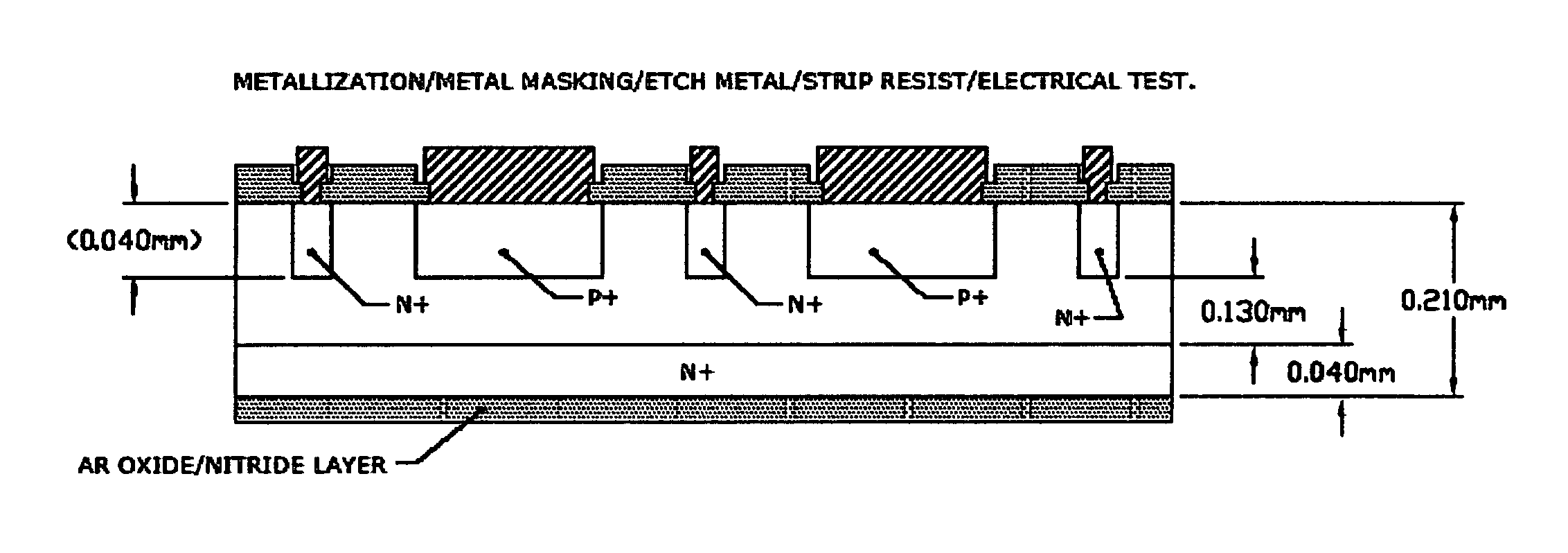
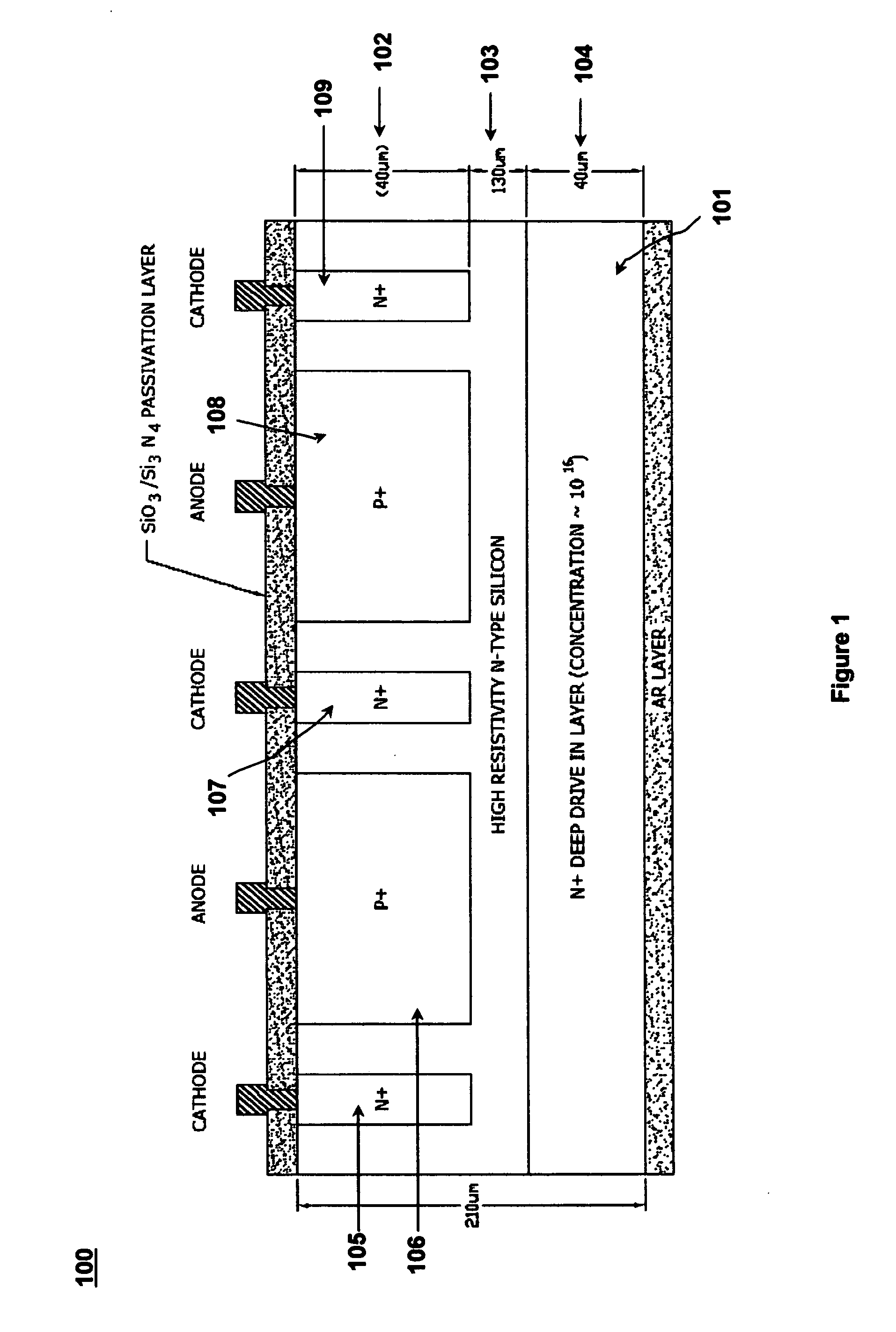
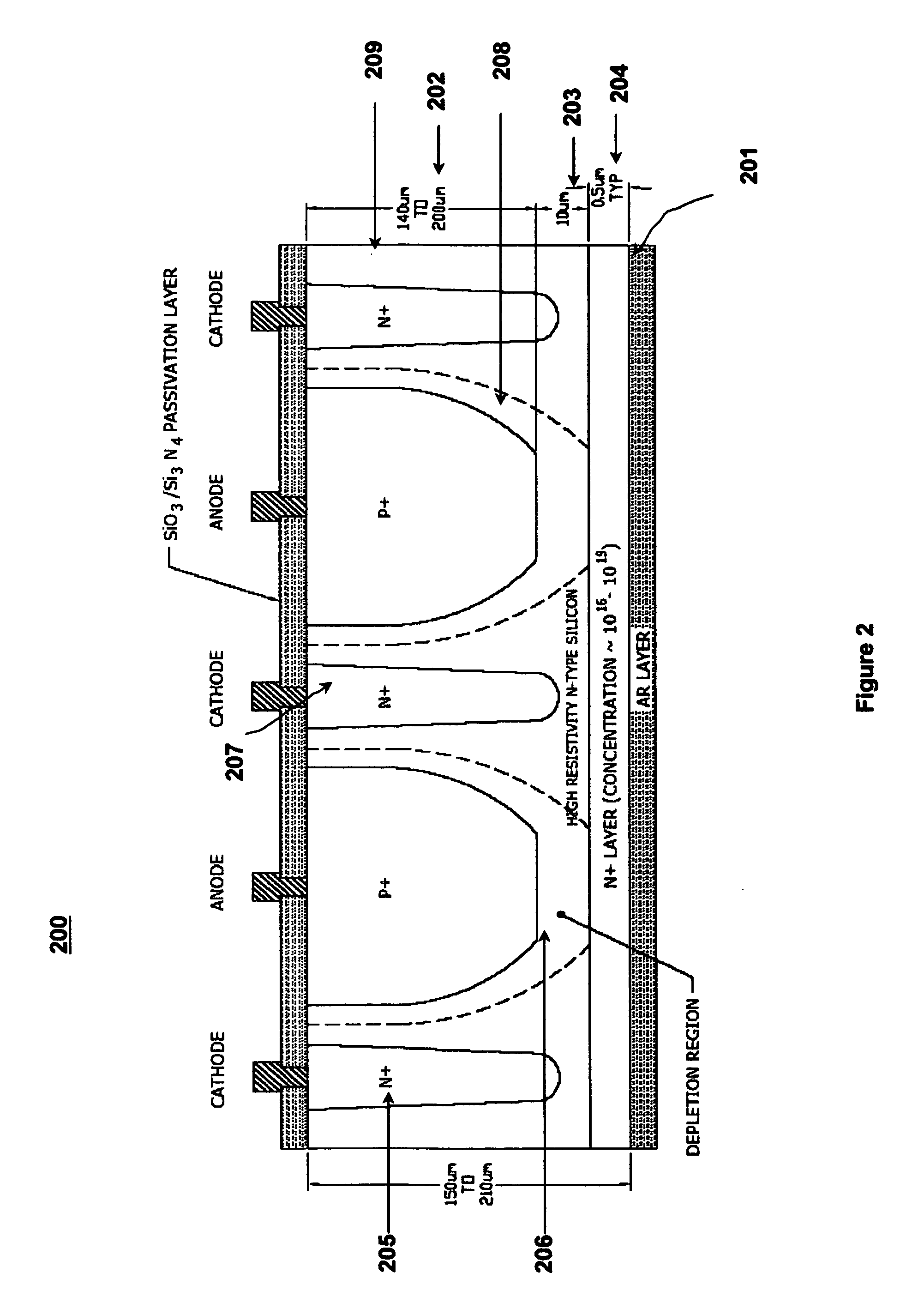
[0022] The invention described herein comprises a plurality of photodiodes, optionally organized in the form of an array, including p+ deep diffused regions or p+ and n+ deep diffused regions. The photodiode arrays have an assortment of beneficial performance characteristics, including, but not limited to, low cost, being economically, technically, and operationally feasible, having high sensivity with low cross talk, and use of reasonably thin, large diameter wafers.

[0023] More particularly, the current invention is a photodiode array having a substrate with at least a front side, and a back side and a plurality of photodiodes integrally formed in the substrate forming the array. Starting from the front side, each photodiode has a passivation layer comprising, for example, SiO2 / Si3N4, and an active high resistivity layer comprising, for example, n-type silicon. The active high resistivity layer comprises at least five regions of alternating conductivity type. In one embodiment, th...


PUM


Abstract

This invention comprises photodiodes, optionally organized in the form of an array, including p+ deep diffused regions or p+ and n+ deep diffused regions. More specifically, the invention permits one to fabricate thin 4 inch and 6 inch wafer using the physical support provided by a n+ deep diffused layer and / or p+ deep diffused layer. Consequently, the present invention delivers high device performances, such as low crosstalk, low radiation damage, high speed, low leakage dark current, and high speed, using a thin active layer.

Description

FIELD OF THE INVENTION [0001] The present invention is directed toward thin wafer photodiodes having improved strength and handling characteristics. Specifically, the present invention is directed towards novel photodiodes, applications using novel photodiodes and methods of making novel photodiodes having a deep diffused p+ region. BACKGROUND OF THE INVENTION [0002] Photodiodes comprise a plurality of electrode radiation-sensitive junctions formed in semiconductor material. Within a photodiode, charge carriers are created by light that illuminates the junction and reverse current is generated that varies with illumination. Photodiodes are used for detection of optical power and subsequent conversion of the same to electrical power. Operationally, photodiodes absorb charged particles, which facilitate detection of incident optical power, thereby generating current proportional to the incident power. [0003] Photodiodes are typified by the quantification of certain characteristics, su...

Claims


Application Information

Patent Timeline
Patent Type & Authority Applications(United States)
IPC IPC(8): H01L29/74H01L29/423H01L31/111
CPCH01L27/1446H01L31/0352H01L31/103
Inventor BUI, PETER STEVENTANEJA, NARAYAN DASS
Owner OSI OPTOELECTRONICS
Why Eureka
Try Eureka