
Modular radiation detector with scintillators and semiconductor photodiodes and integrated readout and method for assembly thereof

a module radiation detector and semiconductor photodiode technology, applied in the field of radiation detection, can solve the problems of inability to measure the point of interaction along this axis using conventional techniques, difficult to relate signals from a compton scattered event to their signals,

Inactive Publication Date: 2007-05-03
GAMMA MEDICA - IDEAS NORWAY
View PDF17 Cites 32 Cited by
  • Summary
  • Abstract
  • Description
  • Claims
  • Application Information

AI Technical Summary

Benefits of technology

[0039] By such means, the invention also reduces the overall volume, and weight of the tomograph compared with the use of photo-multipliers and allows dense packaging of detection modules where each module has small crystal size. The cost per channel for photodiodes is less than the cost per channel for photo-multipliers. The invention improves reliability, and stability over photo-multiplier readout, and can operate in electromagnetic fields and in particular in strong static magnetic fields such as in MRI / NMR instrumentation. A PET combined with MRI / NMR appears technically feasible. Similar application using photo-multipliers was proposed in reference [14]. Operation in a strong static magnetic field reduces the positron travel distance in tissue and thereby improving the spatial resolution. The areas of use are human full body PET, human brain PET, any kind of PET functional imaging in humans and animals. Magnetic fields can be used with silicon photodiodes thus allowing the PET to be combined with MRI instrumentation and opening a new area of multi-modality imaging.
[0043] 3. Detection mode-2: Gamma radiation interacts in the photo-diode arrays. The charge signal from this interaction is measured directly by the photo-diodes in the readout circuit. For 511-keV the main mode of interaction in silicon photo-diodes is Compton scattering where the signal in the photo-diode is created by means of a Compton electron. Depending on the application one can chose to measure the energy of the Compton electron. By measuring the energy of the Compton electron, spatial resolution can be improved [15].
[0050] 8. Scintillator readout option-2: Two sides of the scintillator array are optically connected to two photodiode arrays. The scintillator array is in between two photodiode arrays. The scintillator light splits between the two photodiode arrays. In this option one measures the position of interaction along the crystal using the signal amplitudes from both sides. This option is useful for long crystals corresponding to thick scintillator arrays. Thick scintillator arrays may be employed to reduce the number of readout channels for the tomographic instrument.
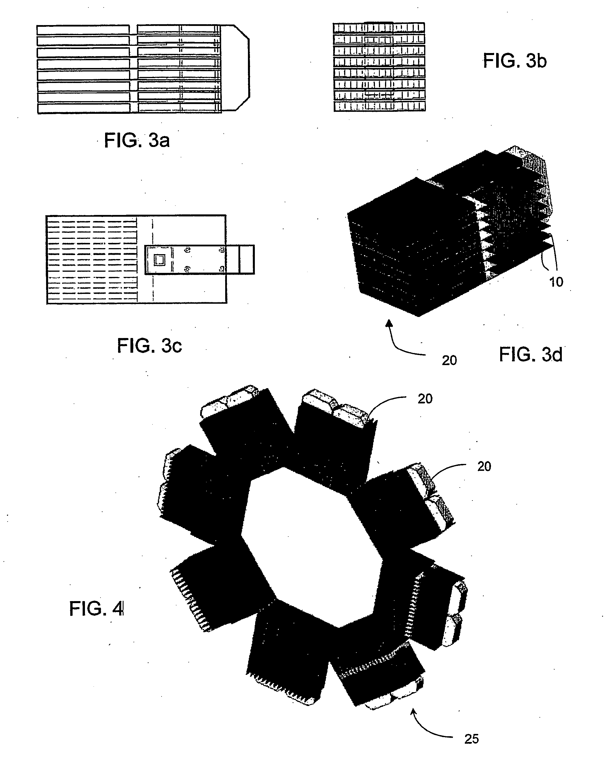
[0054] 12. A scintillator array, a photodiode array, and an ASIC form a radiation detection module. Several radiation detection modules are stacked above each other to form a radiation detection assembly. A tomograph is assembled out of such assemblies in the form of a conventional polygon ring (a part of an annulus) or in the form of a cylinder. The assemblies are oriented with each scintillator array edge-on facing inside the tomograph and electronics facing outside the tomograph. The orientation of the scintillator array allows the depth-of-interaction to be measured.
[0055] 13. The scintillator crystals are glued with an epoxy material. Also disposed on all surfaces of each scintillator crystal, except the surface that bounds the photodiode array, are reflecting layers that are directed inward to the respective scintillator crystal and serve to reflect light into the photodiodes. The non-reflecting outer surface of the reflecting layer allows photons to pass therethrough, but blocks light from exiting from the scintillator crystal apart from through the single exposed surface adjacent to the photodiode array. This reduces cross talk between adjacent scintillator crystals, which would otherwise occur if light produced by a first scintillator crystal could exit and re-enter a second scintillator crystal, thus being detected by an incorrect photodiode. The amount of material in between the scintillator crystals and the amount of material in between detection modules is kept to a minimum. The material in between crystals prevents light cross talk and mechanically keeps crystals in place. The material between modules is constituted by the photo-diode array and its carrier board and both of them can be designed very thin compared to the scintillator array. The modules are arranged along the axis of symmetry of the cylinder, along which axis the crystal pitch can be preserved across all modules.

Problems solved by technology

Signals from a Compton scattered event are difficult to relate to its first point of interaction and the positions measured are blurred.
However, the point of interaction along this axis cannot be measured using conventional techniques.
This is the problem of the missing depth-of-interaction in PET.
The spatial resolution in the tomographic image is ultimately limited by the distance between creation and annihilation of positrons in the tissue.
However, such detector modules still currently suffer from the drawback that in use they provide no indication of depth of interaction of an incoming photon.
There are new scintillator materials with fast and high light output [11], however, the wavelength of emission does not ideally match custom photodiodes.
Moreover, when several such detector modules are stacked to form a detector assembly, the thickness of the ASIC constitutes a dead space between adjacent detector modules that is insensitive to incoming photons.
Present PET instrumentation does not exploit the limits of spatial resolution and detection efficiency as they are set by fundamental physics such as acollinearity of annihilation photons, the finite positron travel path in tissue, and Compton scattering in the tissue.
Existing instrumentation has technical limitations such as missing information of depth-of-interaction, limits in intrinsic spatial resolution, and drawbacks inherent to photo-multipliers such as volume, weight, cost per channel, reliability, stability, signal uniformity, and susceptibility to electro-magnetic fields.

Method used


Image

  • Modular radiation detector with scintillators and semiconductor photodiodes and integrated readout and method for assembly thereof
  • Modular radiation detector with scintillators and semiconductor photodiodes and integrated readout and method for assembly thereof
  • Modular radiation detector with scintillators and semiconductor photodiodes and integrated readout and method for assembly thereof

Examples


Embodiment Construction

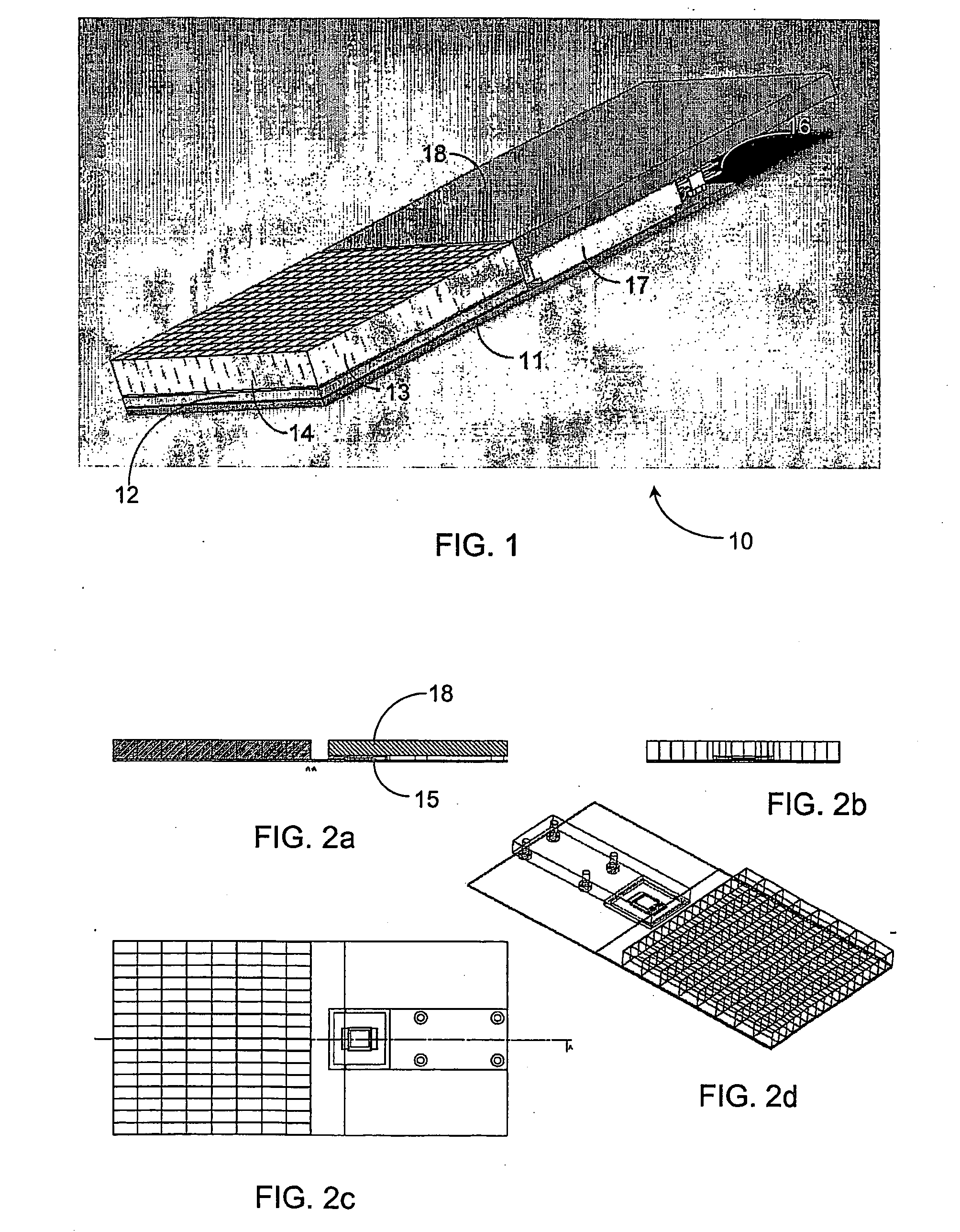
[0066] The drawings illustrate examples of a radiation detection module, and the arrangement of several modules in a package, and the arrangement of several packages in a polygon and cylinder. Specifically, the drawings show the assembly of scintillator arrays and photodiode arrays and readout ASICs with respect to each other. The number of crystals and their aspect ratio are shown as an example, and choices can be made depending on the application and requirements.

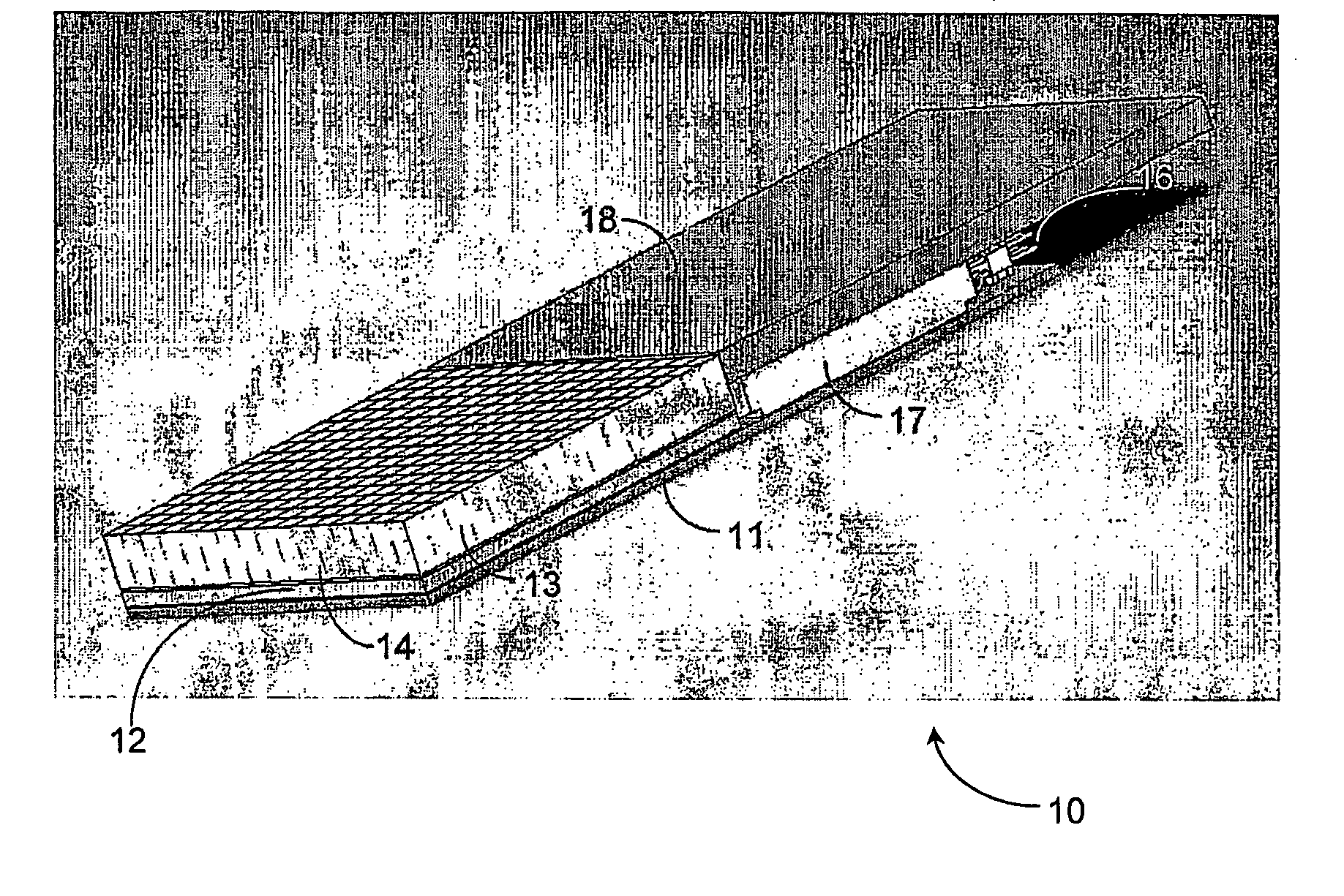
[0067]FIGS. 1 and 2a to 2d show respectively pictorial and schematic representations of a detector module depicted generally as 10 having a carrier board 11 on which is mounted a planar silicon photo-diode array 12 juxtaposed to an upper surface of which is mounted a planar scintillator array 13. An exposed edge 14 of the first row of scintillator elements constitutes a first edge of the scintillator array through which photons striking the detector module propagate through successive scintillator elements of the scintil...


PUM


Abstract

A modular radiation detector (10) with scintillators (13) and semi-conductor photodiodes (12) and integrated readout (15) can be used in positron emission tomography (PET) for functional imaging of humans and animals. Spatial resolution is improved by measuring the depth-of-interaction and modules using photodiodes and integrated readout circuits according to the invention instead of photo-multipliers give rise to lighter and less bulky tomographic instruments. The invention uses very large scale integrated (VLSI) electronic readout circuits for measuring signals from photo-diodes. The electronic readout circuits (15) are located on the module and allow data to be measured and processed at very high rates on the module level rather than on the system level. The use of photodiodes promises greater stability during operation and improved reliability over photo-multipliers. The invention can be used in magnetic fields and therefore allows PET and MRI / NMR imaging techniques to be combined.

Description

FIELD OF THE INVENTION [0001] This invention relates to detecting radiation and measuring (imaging) its distribution in living objects. The invention can be applied in positron emission tomography (PET) where functional images are measured from patient objects. The invention describes a radiation detection module with a scintillator crystal array; and a photo-diode array, and integrated readout electronics. The invention also describes the modular assembly method (packaging in modules) and the arrangement of same in a tomographic imaging instrument. REFERENCES [0002] [1] C. Moisan et al “Segmented LSO Crystals for Depth of Interaction Encoding in PET”, IEEE, Nucl. Sci. Symp. vol. 2, 1112-1116, 1997. [0003] [2] R. S. Miyaoka et al. “Design of Depth of Interaction PET Detector Module”, IEEE, Trans. Nucl. Sci., 45(3):1069-1073, 1998. [0004] [3] W. W. Moses et al. “Performance of a PET Detector Module Utilizing an Array of Silicon Photodiodes to Identify the Crystal of Interaction”, IEE...

Claims


Application Information

Patent Timeline
IPC IPC(8): G01T1/24G01T1/164G01T1/20G01T1/29
CPCG01T1/1644A61B6/037G01T1/2985G01T1/2018G01T1/20183G01T1/20185G01T1/20181G01T1/20182G01T1/20188
Inventor MEIER, DIRKSUNDAL, BJORN M.
Owner GAMMA MEDICA - IDEAS NORWAY
Learn More