

Semiconductor laser device that has the effect of phonon-assisted light amplification and method for manufacturing the same
a laser device and phonon technology, applied in semiconductor devices, lasers, laser details, etc., can solve the problems of inability to easily integrate cannot meet the requirements of the market, etc., to achieve simple structure, facilitate commercialization, and enhance light emission efficiency
- Summary
- Abstract
- Description
- Claims
- Application Information
AI Technical Summary
Benefits of technology
Problems solved by technology
Method used
Image

Examples
Embodiment Construction
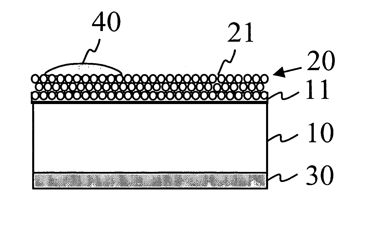
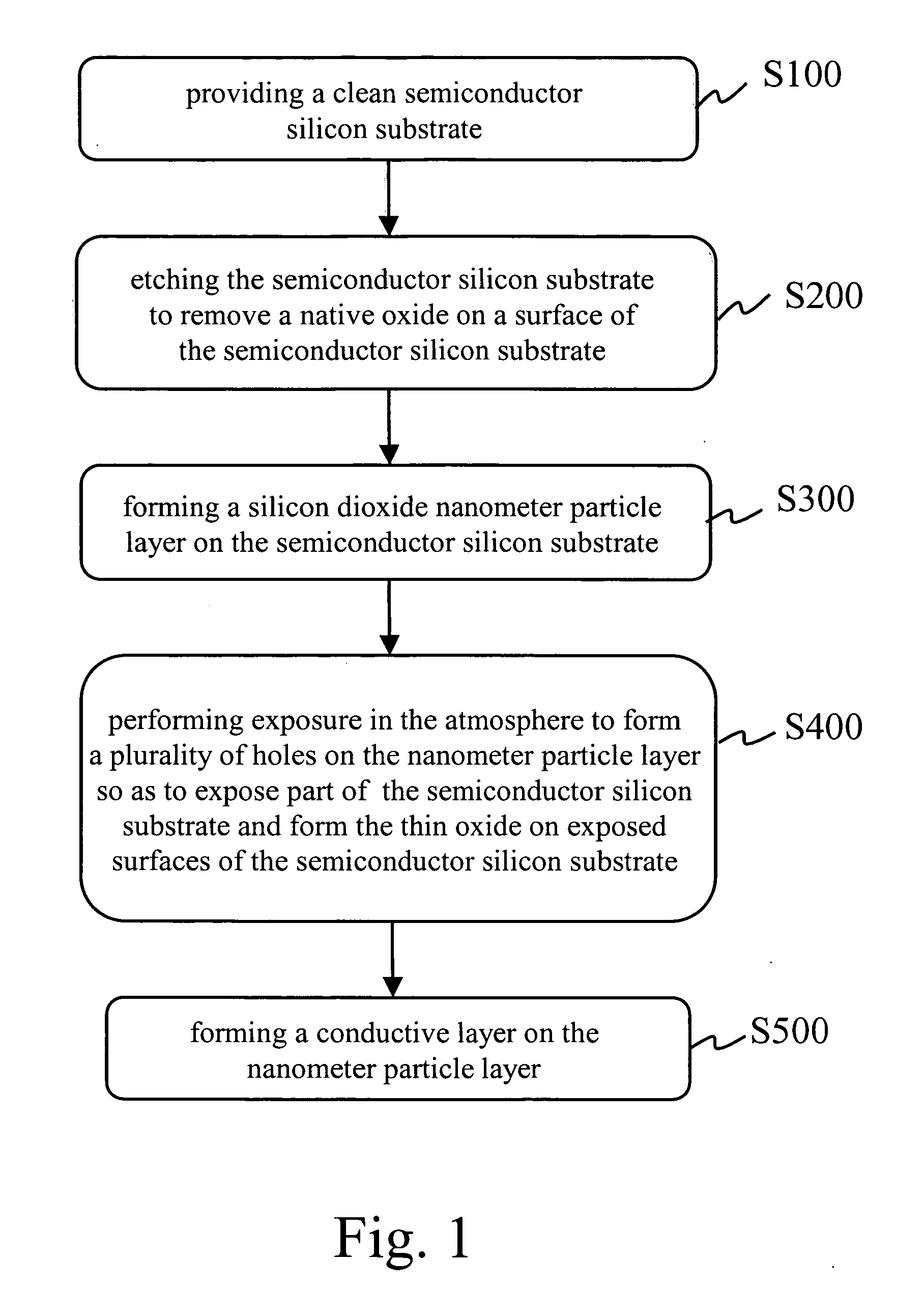
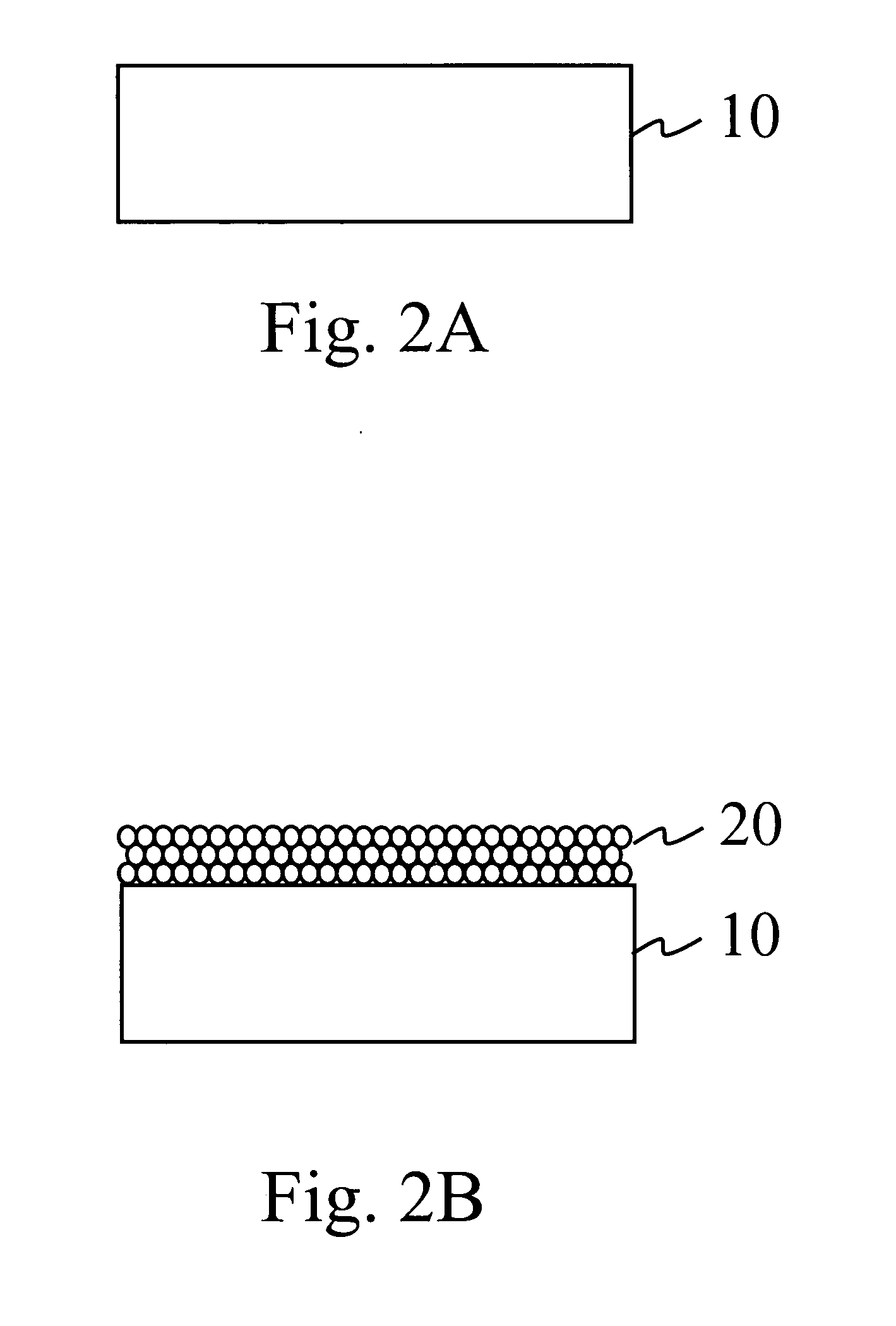
[0020] The present invention provides a semiconductor laser device that has the effect of phonon-assisted light amplification and a method for manufacturing the same, which makes use of the DC-operated phonon-assisted light amplification technique corresponding to silicon energy gap at room temperature. The phonon-assisted stimulated emission mechanism of silicon material is similar to the stimulated Raman scattering mechanism, both emitting photons and phonons. The stimulated Raman scattering, however, absorbs a high-energy photon to emit a lower-energy photon and phonon. The phonon-assisted stimulated emission emits photons and phonons through the recombination of electron-hole pair. Moreover, the phonons generated by the phonon-assisted light emission are at the band edge because of the momentum difference between electron and hole. The present invention utilizes nanometer particles to provide carrier confinement so that injected electrons and holes can easily form excitons at th...
PUM
 Abstract
Description
Claims
Application Information