
Method and Structure for Integrated Solar Cell LCD Panel

a solar cell and lcd panel technology, applied in light radiation electric generators, generators/motors, instruments, etc., can solve the problems of cell phone dead batteries, power consumption increase, and cell phone battery life bottleneck, and achieve the effect of high fill ratio of lcd pixels

Inactive Publication Date: 2007-05-10
XIAI CHARLES YANG
View PDF4 Cites 85 Cited by
  • Summary
  • Abstract
  • Description
  • Claims
  • Application Information

AI Technical Summary

Benefits of technology

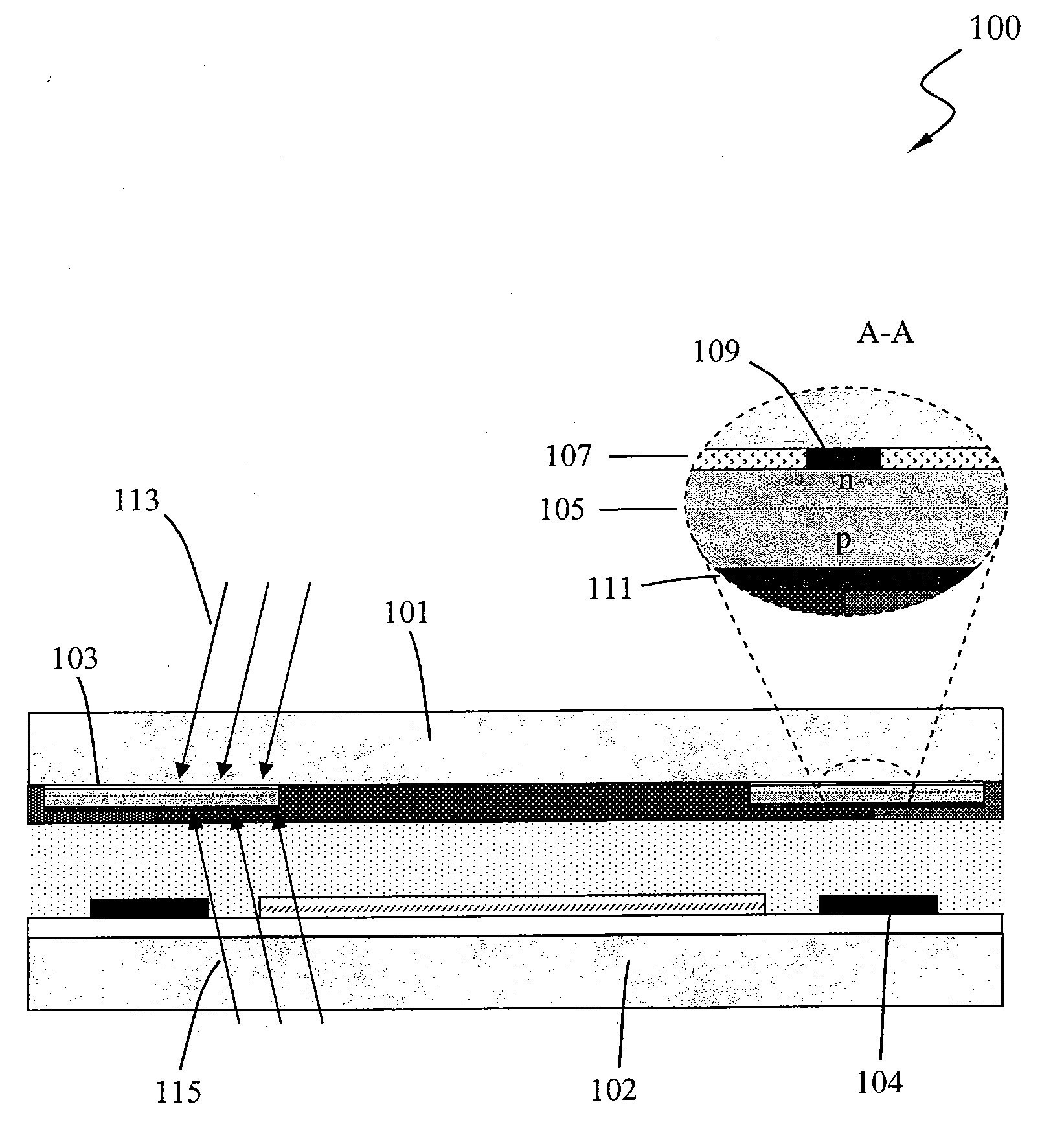
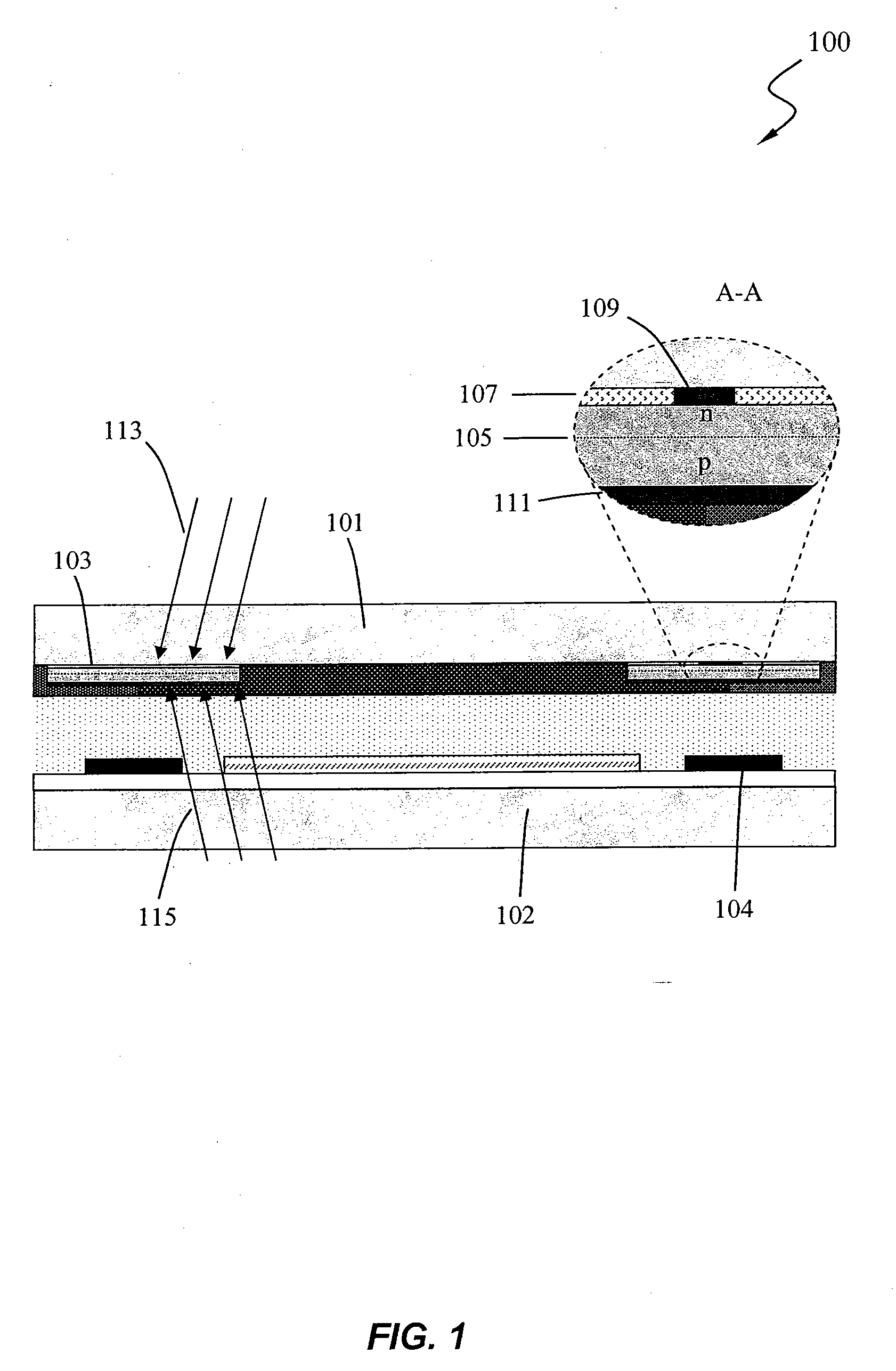
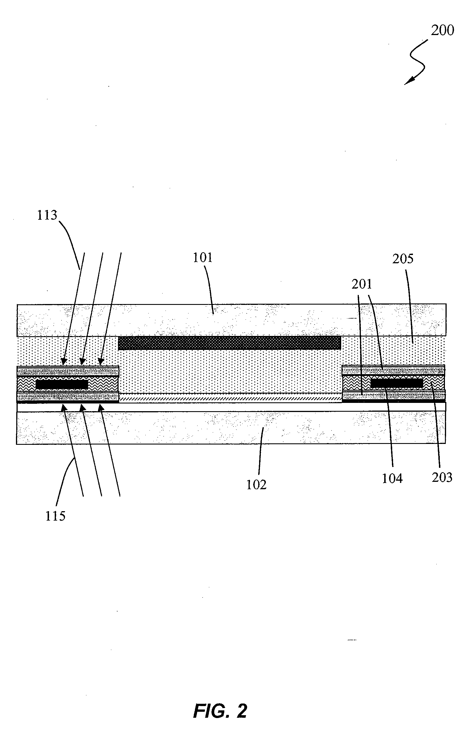
[0005] According to a specific embodiment of the present invention, a lens array substrate is coupled between the light source layer and the TFT substrate. A micro lens collects the backlight within a pixel cell and focuses the light with the focal point or the beam waist at the solar cell layer. As a result, a larger solar cell area is applied to absorb more ambient light while maintaining high fill ratio of the LCD pixels.

Problems solved by technology

As more features such as music and video added to cell phones, power consumption increases significantly.
Battery life becomes a bottleneck.
Furthermore, dead batteries in cell phones cause inconvenience and have safety concerns in an emergency situation.
Commercially available stand-alone solar panel for charging portable electronic devices is bulky and cumbersome; therefore it has not been adopted widely by consumers.

Method used


Image

  • Method and Structure for Integrated Solar Cell LCD Panel
  • Method and Structure for Integrated Solar Cell LCD Panel
  • Method and Structure for Integrated Solar Cell LCD Panel

Examples


Embodiment Construction

[0011] According to the present invention, techniques for manufacturing objects are provided. More particularly, the invention provides a method and device for fabricating an out-of-plane compliant micro actuator. The method and device can be applied to LCD panels as well as other devices, for example, sensors, detectors, and optical systems.

[0012] As illustrated in Prior Art diagrams, a conventional LCD panel has a black matrix on the color filter substrate covers data bus-line and TFT (not shown) regions and blocks both ambient light and backlight from reflecting back to outside. As a result, aperture ratio ranges from 50% to 70% for typical LCD panels. The remaining 30% to 50% panel area is covered by the black matrix.

[0013]FIG. 1 is a simplified cross section diagram illustrating components of integrated solar cell LCD panel according to one embodiment of the present invention. As illustrated, the black matrix on the color filter substrate 101 is replaced by solar cells 103. T...


PUM


Abstract

The present invention relates to a method and device for integrating solar cell on LCD panels for photovoltaic electricity generation for portable electronic devices. According to one embodiment of the present invention, the black matrix region on the color filter substrate in a LCD panel is replaced by a solar cell region. A lens array substrate is coupled between the light source layer and the TFT to focus the backlight to increase the solar cell layer area while maintaining high fill ratio of the LCD pixels. The solar cell material is selected from at least silicon, a single crystal silicon, poly-crystalline silicon, amorphous silicon, gallium arsenide, cadmium telluride, copper indium diselenide, organic / inorganic, or hybrid cells. The substrate material is selected from glass, metal, plastic or polymer.

Description

[0001] This application claims priority to provisional application Ser. No. 60 / 732,388; filed on Oct. 31, 2006; commonly assigned, and of which is hereby incorporated by reference for all purposes.BACKGROUND OF THE INVENTION [0002] Portable electronics devices such as cell phones become indispensable part of daily life. As more features such as music and video added to cell phones, power consumption increases significantly. Battery life becomes a bottleneck. Furthermore, dead batteries in cell phones cause inconvenience and have safety concerns in an emergency situation. Commercially available stand-alone solar panel for charging portable electronic devices is bulky and cumbersome; therefore it has not been adopted widely by consumers. Thus, there is a need in the art for methods and apparatus for fabricating an integrate solar cell devices on LCD panel for photovoltaic electricity generation for portable electronic devices. SUMMARY OF THE INVENTION [0003] According to the present i...

Claims


Application Information

Patent Timeline
IPC IPC(8): H02N6/00
CPCG02F1/133512G02F2001/13324G02F2001/133562G02F2001/133565H01L31/0296H01L31/03682H01L31/0543H01L31/0749Y02E10/52Y02E10/541Y02E10/548Y02E10/546H01L31/03762G02F1/13324G02F1/133565G02F1/133562
Inventor YANG XIAO (CHARLES)
Owner XIAI CHARLES YANG
Learn More