

P-type group ii-vi semiconductor compounds
a semiconductor compound and iivi technology, applied in the direction of crystal growth process, polycrystalline material growth, chemically reactive gas, etc., can solve the problems and achieve the effect of inhibiting single crystal formation and reducing desired electronic properties
- Summary
- Abstract
- Description
- Claims
- Application Information
AI Technical Summary
Benefits of technology
Problems solved by technology
Method used
Image

Examples
example 1
Sputtering of ZnO with Arsenic as a Dopant
[0060] A thin film of p-type zinc oxide was deposited onto a self supporting substrate by RF sputtering. Both fused silica and silicon wafers were used as the self supporting substrate. The sputtering target composition was ZnO (0.99−0.95 moles)+As (0.01−0.05 moles). The preferred target composition was ZnO (0.98 moles)+As (0.02 moles). The substrate temperature was between 350 and 550° C. The preferred temperature was about 400° C. The RF power was between 20 and 120 watts. The preferred power was about 60 watts. The sputtering atmosphere included argon at a gas pressure of about 4 to 20 mtorr and O2 at a gas pressure of about 1 to 4 mtorr. The preferred sputtering atmosphere pressures were about 9 mtorr argon and about 1 mtorr O2.
[0061] The resulting transparent p-type zinc oxide layer had a resistance of about 10,000 ohms / square. After annealing at 440° C. in air, the resistance dropped to about 1,000 ohms / square. In another composition...
example 2
Sputtering of ZnO with Arsenic as a Dopant
[0062] A thin film of p-type zinc oxide was deposited onto a self supporting substrate by RF sputtering. Both fused silica and silicon wafers were used as the self supporting substrate. The sputtering target composition was ZnO (0.99−0.95 moles)+As (0.01−0.05 moles). The preferred target composition was ZnO (0.98 moles)+As (0.02 moles). The substrate temperature was between 350 and 550° C. The preferred temperature was about 400° C. The RF power was between 20 and 120 watts. The preferred power was about 60 watts. The sputtering atmosphere included argon at a gas pressure of about 4 to 20 mtorr and H2 at a gas pressure of about 1 to 4 mtorr. The preferred sputtering atmosphere pressures were about 9 mtorr argon and about 1 mtorr H2.
[0063] The resulting transparent p-type zinc oxide layer had a resistance of about 500 ohms / square. Without being bound by theory, it is believed that the hydrogen gas may be moderating the concentration of oxyg...
example 3
Sputtering of ZnO with Arsenic as a Dopant
[0064] A thin film of p-type zinc oxide was deposited onto a self supporting substrate by RF sputtering. Both fused silica and silicon wafers were used as the self supporting substrate. The sputtering target composition was ZnO (0.99−0.95 moles)+As (0.01−0.05 moles). The preferred target composition was ZnO (0.975 moles)+As (0.025 moles). The substrate temperature was between 350 and 550° C. The preferred temperature was about 400° C. The RF power was between 20 and 120 watts. The preferred power was about 60 to 90 watts. The sputtering atmosphere included argon at a gas pressure of about 4 to 20 mtorr. The preferred sputtering atmosphere pressure was about 9 mtorr argon.
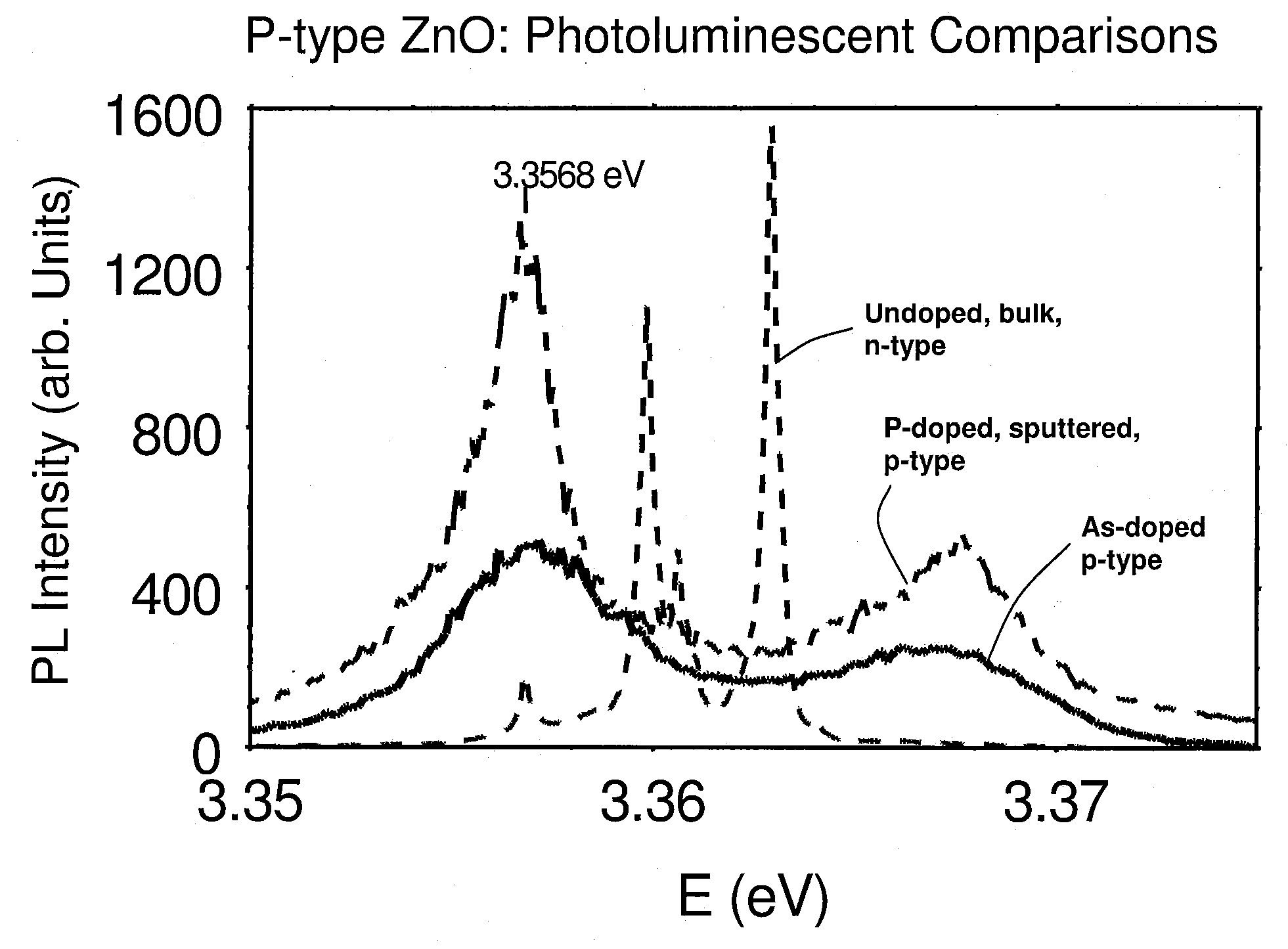
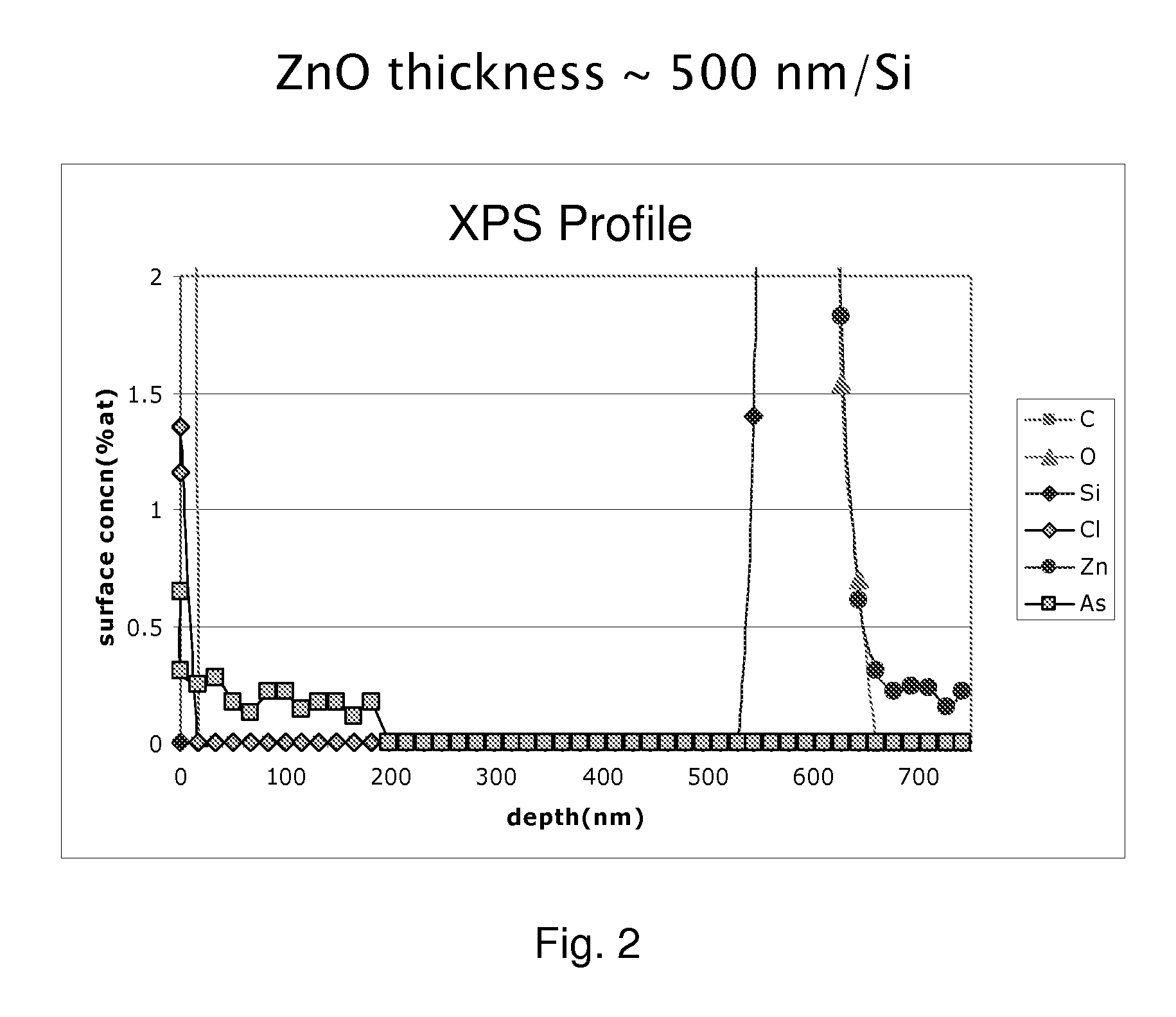
[0065] The resulting transparent p-type zinc oxide layer had a resistance of about 1000 ohms / square. The resulting p-type zinc oxide was analyzed by X-ray Photoelectron Spectroscopy (XPS). A graph of the XPS data is shown in FIG. 2. The data from FIG. 2 show arsenic in zin...
PUM
| Property | Measurement | Unit |
|---|---|---|
| carrier mobility | aaaaa | aaaaa |
| semiconductor resistivity | aaaaa | aaaaa |
| resistivity | aaaaa | aaaaa |
Abstract
Description
Claims
Application Information