Switching device

a technology of switching device and switch, which is applied in the direction of thermoelectric devices, instruments, nanoinformatics, etc., can solve the problems of affecting the bistable performance of the device as a whole, the proportion of the two components is critical, and the switch device uses an organic charge transfer complex. achieves stable bistable performance, suppresses material composition variation, and excellent bistable characteristics

Inactive Publication Date: 2007-05-17
SHARP KK
View PDF1 Cites 2 Cited by
  • Summary
  • Abstract
  • Description
  • Claims
  • Application Information

AI Technical Summary

Benefits of technology

[0021] These quinone compounds exhibit excellent characteristics for bistable characteristic because of high ratio of the resistance in the high resistance state / the resistance in the low resistance state. Therefore, the quinone compounds can be favorably used for an organic bistable material.
[0022] The present invention suppresses variation in material composition and provides a steady bistable performance, and thus provides a switching device suitable for mass production and exhibiting good repetition performance. Therefore, the switching device can be used for a driver switching device of organic EL display panels and for high density memories.

Problems solved by technology

The switching devices using an organic charge transfer complex mentioned above, however, had the problems described in the following.
Therefore, any excess or deficiency in the proportion of the two components critically affects the bistable performance of the device as a whole.
It is particularly difficult to obtain a large area and uniform film when using film deposition by means of vacuum evaporation, due to differences in vapor pressure of the two components and, in the case of co-evaporation, geometric arrangement of the individual evaporation source for each material.
Therefore, it is difficult to mass produce switching devices that perform with a steady bistability characteristic and uniform quality from the conventional organic bistable materials of two-component systems.

Method used


Image

  • Switching device
  • Switching device
  • Switching device

Examples


example 1

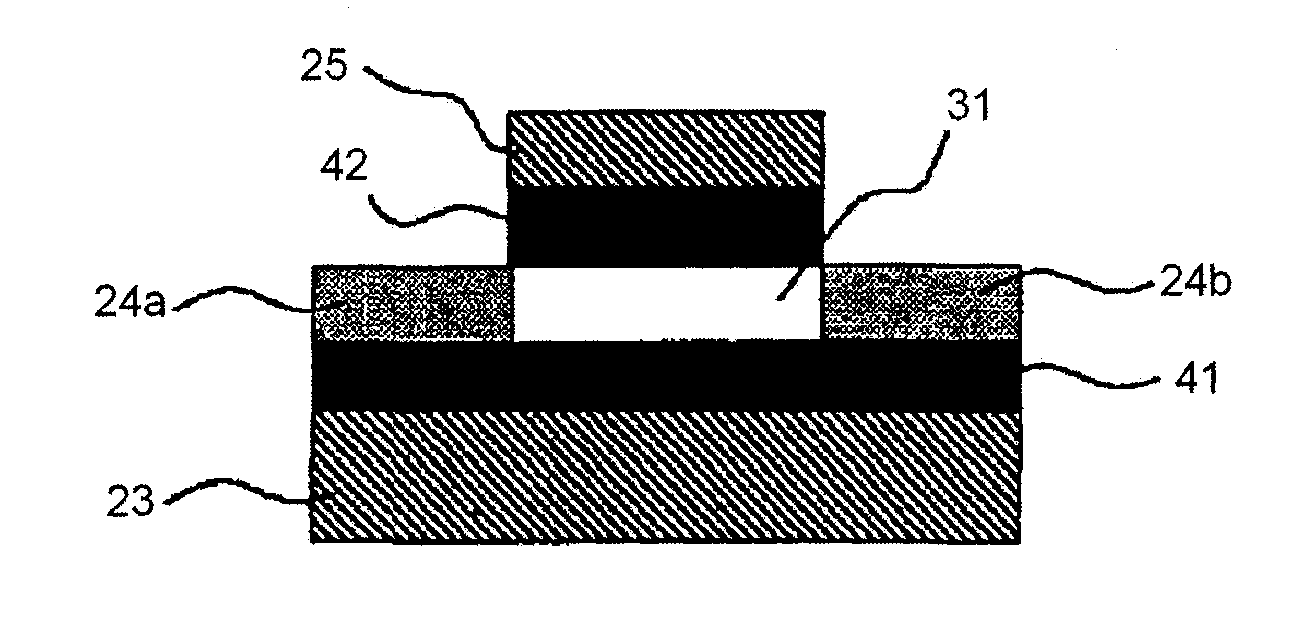
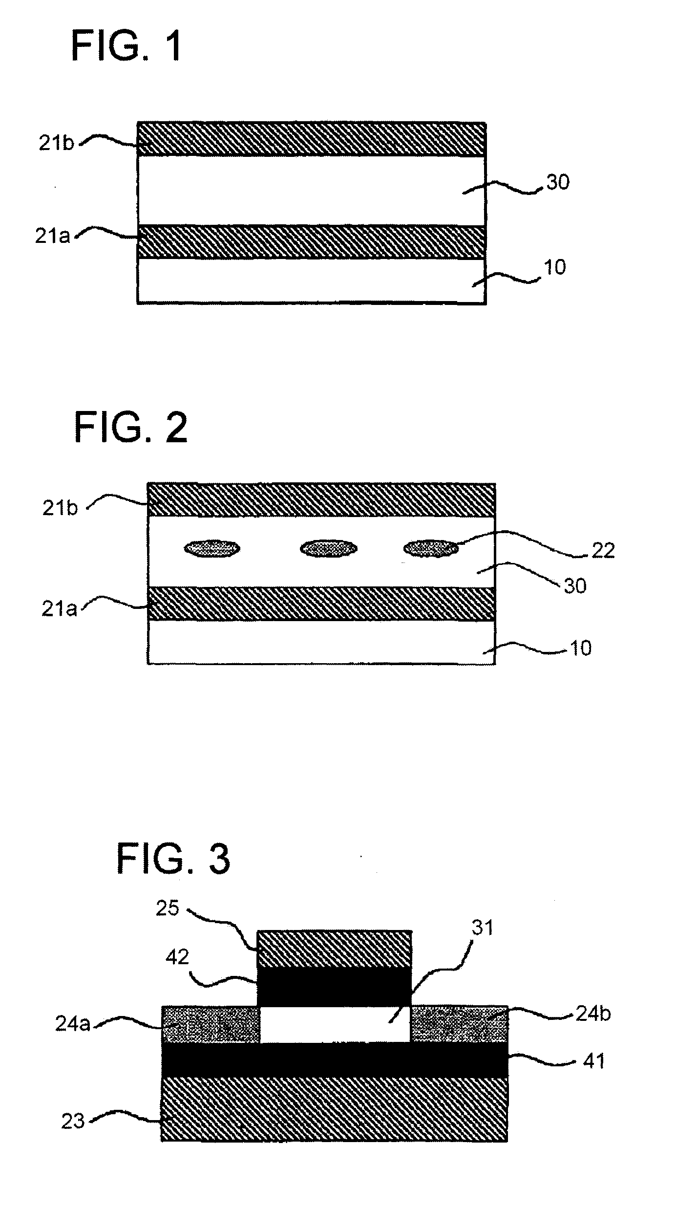
[0074] A switching device having a structure of FIG. 1 was produced in the following procedure. A glass substrate was used for substrate 10. Thin films of first electrode layer 21a, organic bistable material layer 30, and second electrode layer 21b having thicknesses of 100 nm, 80 nm, and 100 nm, respectively, were sequentially formed on the substrate by means of vacuum evaporation method, to form a switching device of Example 1.

[0075] Evaporation sources were aluminum for first electrode layer 21a and second electrode layer 21b, and a quinone compound represented by the structural formula (I-1) for organic bistable material layer 30. The evaporation apparatus was evacuated to 3×10⁻⁶ torr by a diffusion pump. The evaporation of aluminum was conducted by a resistance heating method with a deposition speed of 3 Å / sec; the evaporation of the quinone compound was conducted by a resistance heating method with a deposition speed of 2 Å / sec. The processes of evaporating the layers were co...

example 2

[0076] A switching device was produced in the same manner as in Example 1 except that the organic bistable material represented by the structural formula (I-1) used in Example 1 was replaced by the organic bistable material represented by the structural formula (I-2).

example 3

[0077] A switching device was produced in the same manner as in Example 1 except that the organic bistable material represented by the structural formula (I-1) used in Example 1 was replaced by the organic bistable material represented by the structural formula (II-1).


PUM

PropertyMeasurementUnit
thicknessaaaaaaaaaa
temperatureaaaaaaaaaa

Abstract

A switching device is discloses that exhibits two stable resistance values to a voltage applied between electrodes. The switching device comprises thin films of a first electrode layer, an organic bistable material layer and a second electrode layer sequentially formed on a substrate, and the organic bistable material is a specified quinone compound.

Description

CROSS REFERENCE TO RELATED APPLICATIONS [0001] This application is a continuing application based on International Application no. PCT / JP2005 / 009182, which claims priority from Japanese application Ser. No. JP 2004-149963 filed on May 20, 2004, the contents of which are incorporated herein in their entirety. BACKGROUND OF THE INVENTION [0002] A. Field of the Invention [0003] The present invention relates to a switching device that can be used for driver switching devices of a display panel using an organic EL or a liquid crystal, and for high density memories. [0004] B. Description of the Related Art [0005] Recently, the performance of organic electronic materials has made spectacular advances. Some low dimensional conductors, such as charge transfer complexes, exhibit a distinctive property, for example, metal-insulator transition, and have been studied for application to driver switching devices of organic EL display panels or to high density memories. [0006] Organic bistable mate...

Claims


Application Information

Patent Timeline
Patent Type & Authority Applications(United States)
IPC IPC(8): H01L29/08C07D487/00C08G61/04G02F1/1365H01L27/10H01L49/02H01L51/00H05B33/14
CPCB82Y10/00G02F1/1365G02F2202/02H01L51/0052H01L51/0062H01L51/0065H01L51/0067H01L51/0068H01L51/0071H01L51/0073H01L51/0074H01L51/0591H01L51/0595H10K85/615H10K85/649H10K85/653H10K85/654H10K85/655H10K85/657H10K85/6574H10K85/6576H10K10/701H10K10/50G02F2202/021H10K30/671H10K10/00
Inventor SEKINE, NOBUYUKIKAWAKAMI, HARUOKATO, HISATOYAMASHIRO, KEISUKEKATO, KYOKOKURODA, MASAMI
Owner SHARP KK
Why Eureka
Try Eureka