Semiconductor device and method of fabricating the same

a technology of semiconductors and semiconductors, applied in the direction of semiconductors, semiconductor devices, electrical equipment, etc., can solve the problems of increased parasitic resistance components, increased junction leakage in pn, and threshold voltage fluctuation

Inactive Publication Date: 2007-05-17
PANASONIC CORP
View PDF1 Cites 146 Cited by
  • Summary
  • Abstract
  • Description
  • Claims
  • Application Information

AI Technical Summary

Benefits of technology

[0110] As has been explained thus far, the present embodiment achieves such advantageous effects as realization of a gate length that is below the processing limit by lithography, reduction in gate fringe capacitance, and moreover attaining a gate structure that is a mushroom structure.
[0111] It should be noted that in the present embodiment as well, a Si bulk substrate may be used in place of the SOI substrate. Moreover, the present embodiment may be modified in similar manners to those in the first and the second modified examples of the first embodiment.
[0112] In the first embodiment and the second embodiment, the layer that has been described as the “SiGeC layer” may be substituted by either one of a SiGe layer, which does not contain C, or a SiC layer, which does not contain Ge.

Problems solved by technology

Making the source / drain high-concentration diffusion layer shallow causes the portion located below the silicide layer of the source / drain high-concentration diffusion layer to have a reduced thickness, resulting in an increase in the parasitic resistance component and an increase in the junction leakage in the pn junction between the source / drain high-concentration diffusion layer and a body region, which originates from the silicide layer.
Nevertheless, formation of the elevated source / drain structure by selective growth has problems such as follows.
When the impurity profile is disordered, variations in the effective gate length and short channel effects occur, causing the threshold voltage to fluctuate.
This, however, creates a problem of lower throughput because the growth rate of low-temperature Si growing is slow.
To enhance the selectivity, addition of a hydrogen chloride gas during the crystal growth is known to be effective; however, the use of a chlorine-based gas may risk corrosion of chamber or piping.
The shape of the facet is difficult to control because it depends on the aperture rate of the mask pattern and the material of the mask in addition to the conditions for the crystal growth.
As discussed above, although the elevated source / drain structure has proved to be effective in improving device performance, the selective growth for forming the elevated source / drain structure has not yet been practical because it has many problems.

Method used


Image

  • Semiconductor device and method of fabricating the same
  • Semiconductor device and method of fabricating the same
  • Semiconductor device and method of fabricating the same

Examples


first embodiment

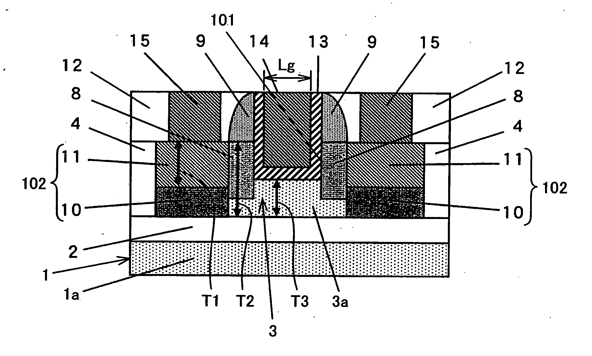
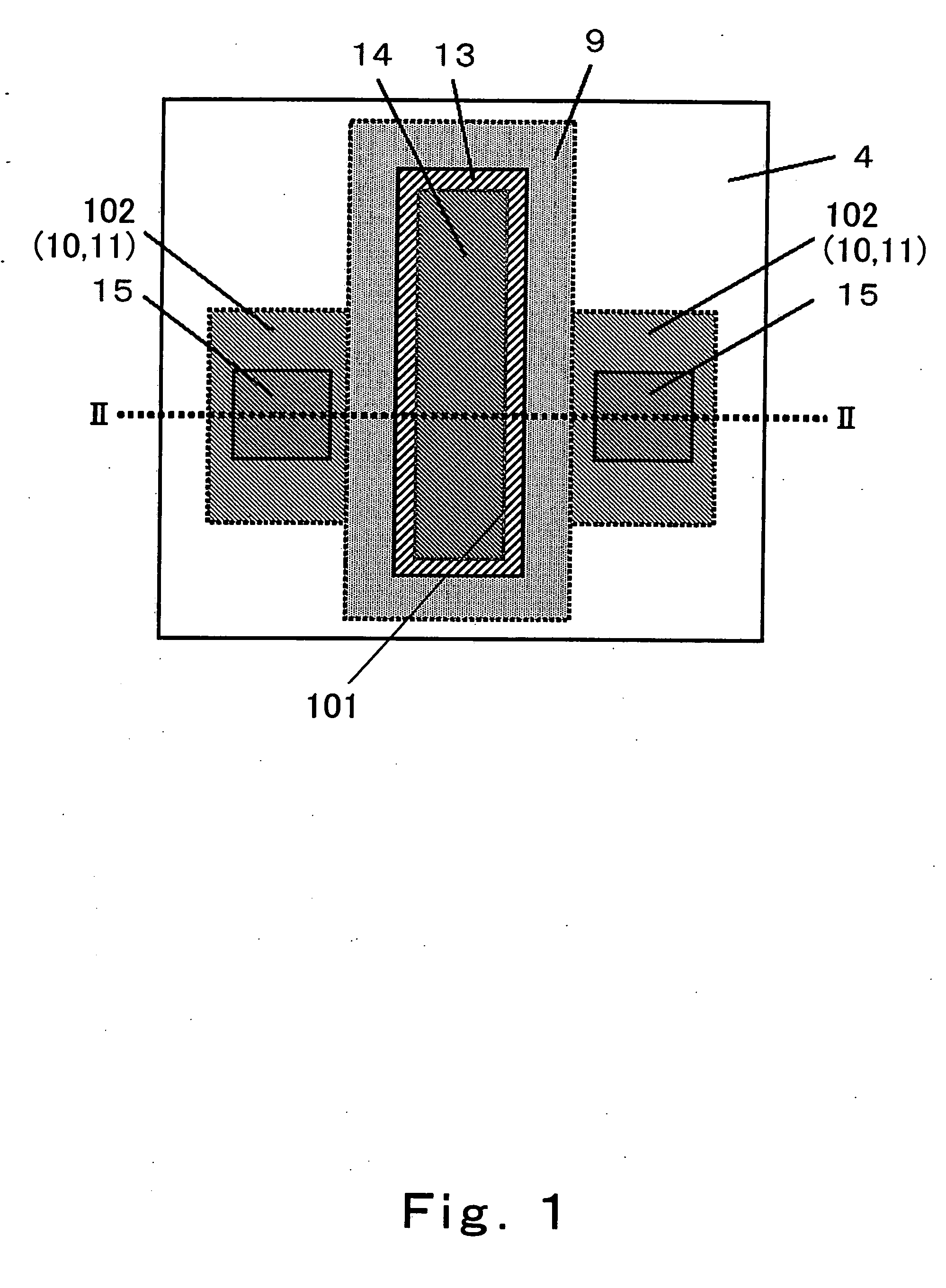
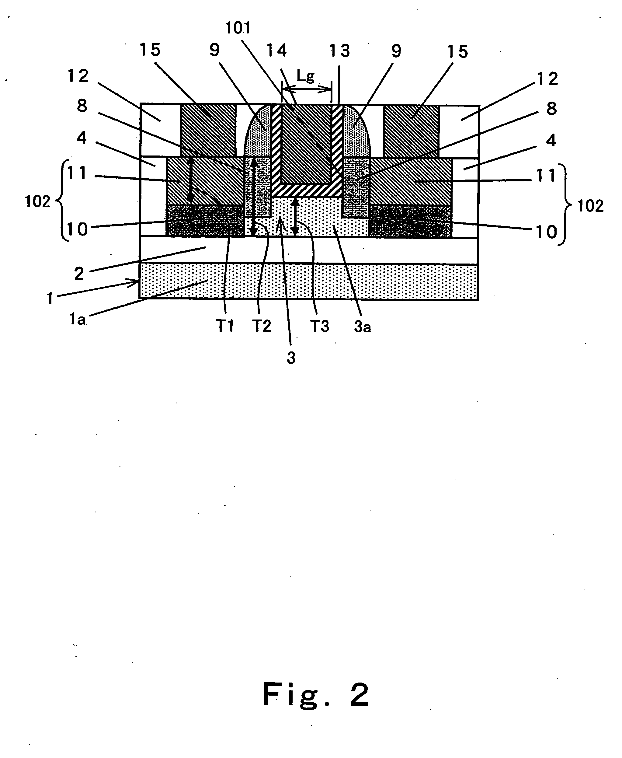
[0049]FIG. 1 is a plan view schematically illustrating the structure of a semiconductor device, viewed in plan, according to a first embodiment of the present invention, and. FIG. 2 is a cross-sectional view taken along line II-II in FIG. 1, schematically illustrating the structure of the semiconductor device, viewed in cross-section, according to the first embodiment of the present invention.

[0050] Herein, the semiconductor device is a n-MISFET. As a substrate 1, an SOI substrate is used.

[0051] Referring to FIGS. 1 and 2, the semiconductor device has a substrate 1. Herein, the substrate 1 is made of an SOI substrate. The SOI substrate 1 is constructed by forming a SiO2 box layer 2 and a Si body layer 3 on a Si substrate 1a in that order. In the present specification, this unprocessed Si body layer in the SOI substrate 1 is referred to as a “Si body layer,” and is represented by reference numeral 3. Various constituent elements of the semiconductor device are constructed within th...

first modified example

[0093]FIG. 5 is a cross-sectional view schematically illustrating a semiconductor device of a first modified example according to the present embodiment.

[0094] As illustrated in FIG. 5, the semiconductor device is formed by a hetero MISFET in the present modified example.

[0095] The hetero MISFET of the present modified example utilizes, as the substrate 1, a substrate in which a SiGeC channel layer 22 and a Si cap layer 23 having a thickness of about about 5 nm to 20 nm are formed successively on a Si substrate 1a using a UHV-CVD (Ultra High Vacuum Chemical Vapor Deposition) method. Then, an insulator 4 is formed so as to reach the Si substrate 1a, and an active region is formed of the Si substrate 1a, the SiGeC channel layer 22, and the Si cap layer 23 that are surrounded by the insulator 4. In the substrate 1, the gate recess 101 is formed in the Si cap layer 23 because the Si cap layer 23 is the uppermost layer. As shown in FIG. 5, when the thickness of the silicide layer 11 is...

second modified example

[0096]FIG. 6 is a cross-sectional view schematically illustrating the configuration of a semiconductor device of a second modified example according to the present embodiment.

[0097] As illustrated in FIG. 6, the semiconductor device is formed by a strained Si MISFET in the present modified example.

[0098] The strained Si MISFET of the present modified example utilizes, as the substrate 1, a substrate in which a relaxed SiGeC layer 24 and a strained Si channel layer 25 having a thickness of about 1 μm to 4 μm are formed successively on a Si substrate 1a using a UHV-CVD method. Then, an insulator 4 is formed in the strained Si channel layer 25, and an active region is formed of a region of the strained Si channel layer 25 surrounded by the insulator 4. In the substrate 1, the gate recess 101 is formed in the strained Si channel layer 25 because the strained Si channel layer 25 is the uppermost layer. As shown in FIG. 6, when the film thickness of the silicide layer 11 is represented ...


PUM


Abstract

A semiconductor device according to the present invention, which comprises a MISFET, has a semiconductor layer (3) having a recessed portion (101) formed in the surface thereof, the recessed portion (101) having an opening the outer circumference of which is closed, a gate insulating film (13) formed so as to cover at least the inner face of the recessed portion (3), a gate electrode (14) filling the recessed portion (101) such that the gate insulating film (13) is interposed between the gate electrode (14) and the inner face of the recessed portion (101), and a pair of source / drains (102), located on both sides of the gate electrode (14) when viewed in plan and formed to a predetermined depth from the surface of the semiconductor layer (3).

Description

RELATED APPLICATION [0001] This application is the U.S. National Phase under 35 U.S.C. § 371 of International Application No. PCT / JP2004 / 006157, filed on Apr. 28, 2004, which in turn claims the benefit of Japanese Application No. 2003-124043, filed on Apr. 28, 2003, the disclosure of which Applications are incorporated by reference herein.TECHNICAL FIELD [0002] The present invention relates to a semiconductor device, and particularly to a MIS transistor having an elevated source / drain structure, in which a source and a drain are formed at higher positions than a gate insulating film. BACKGROUND ART [0003] To date, advancing miniaturization has been the guiding principle to improve the performance of field effect transistors (FETs). For sub-100 nm generation MISFETs (metal-insulator semiconductor FETs), it has been essential that the source / drain high-concentration diffusion layer be made shallow in order to prevent short channel effects and punch-through. Making the source / drain hig...

Claims


Application Information

Patent Timeline
Patent Type & Authority Applications(United States)
IPC IPC(8): H01L29/94H01L21/336H01L29/78H01L29/786
CPCH01L29/66545H01L29/66553H01L29/66621H01L29/66772H01L29/7834H01L29/78621
Inventor INOUE, AKIRATAKAGI, TAKESHISORADA, HARUYUKI
Owner PANASONIC CORP
Why Eureka
Try Eureka