Lateral phase change memory with spacer electrodes and method of manufacturing the same

a technology of spacer electrodes and phase change memory, which is applied in the direction of bulk negative resistance effect devices, electrical apparatus, semiconductor devices, etc., can solve the problems of uniformity and reliability, more power consumption, and difficulty in gap-filling and sidewall contact of phase change materials, so as to reduce the parasitic resistance of the conductive path, increase the heating efficiency, and reduce the contact area

Inactive Publication Date: 2007-05-31
IND TECH RES INST
View PDF11 Cites 17 Cited by
  • Summary
  • Abstract
  • Description
  • Claims
  • Application Information

AI Technical Summary

Benefits of technology

[0015] In view of the above problem, a lateral phase change memory with spacer electrodes and method of manufacturing the same are provided, wherein the spacer electrodes are added at the position of the conductive electrode of the phase change memory acting as heating electrodes, so as to increase the heating efficiency and to reduce the parasitic resistance of the conductive path. The contact area is also reduced by contacting the spacer electrodes with the phase change material laterally. So, the programming current and power consumption of the phase change memory can be reduced. Moreover, with the addition of the spacer electrodes, the gap-filling ability of the phase change material can be improved, and the interface contact quality of the phase change material with the heating electrodes is better as well.

Problems solved by technology

Therefore, the density of the phase change memory can be efficiently increased by reducing the programming current of the phase change memory, which also has become the biggest challenge for the development of the phase change memory technology.
This may result in the gap-filling and sidewall-contacting difficulty of the phase change material as well as the problems of uniformity and reliability.
Further, the current flowing path of the heating electrode with higher resistivity in the phase change memory is relatively long, and the phase change material occupies an excessively large volume in the element; thus, when the current flows form the lateral heating electrode to the upper electrode, more power will be consumed.
Generally, to increase the heating efficiency of the phase change material, a heating electrode material with higher resistivity is required to be used in the phase change memory element, and if the heating electrode is also used as a conductive path in the design, the parasitic resistance will be increased resulting in additional power consumption.
Further, when the distance between the two electrodes has been gradually reduced, it will be more and more difficult for the gap filling of phase change material, thereby resulting in poor interface contact between the lateral electrode and the phase change material, and problems of uniformity and reliability of the element.

Method used


Image

  • Lateral phase change memory with spacer electrodes and method of manufacturing the same
  • Lateral phase change memory with spacer electrodes and method of manufacturing the same
  • Lateral phase change memory with spacer electrodes and method of manufacturing the same

Examples


first embodiment

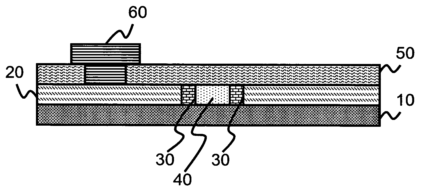
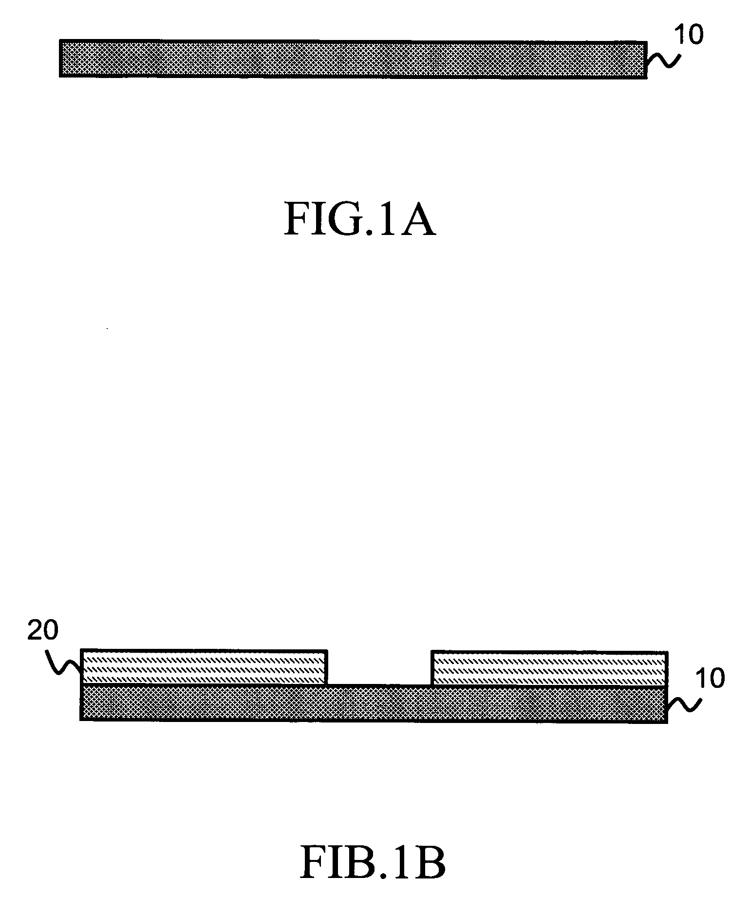
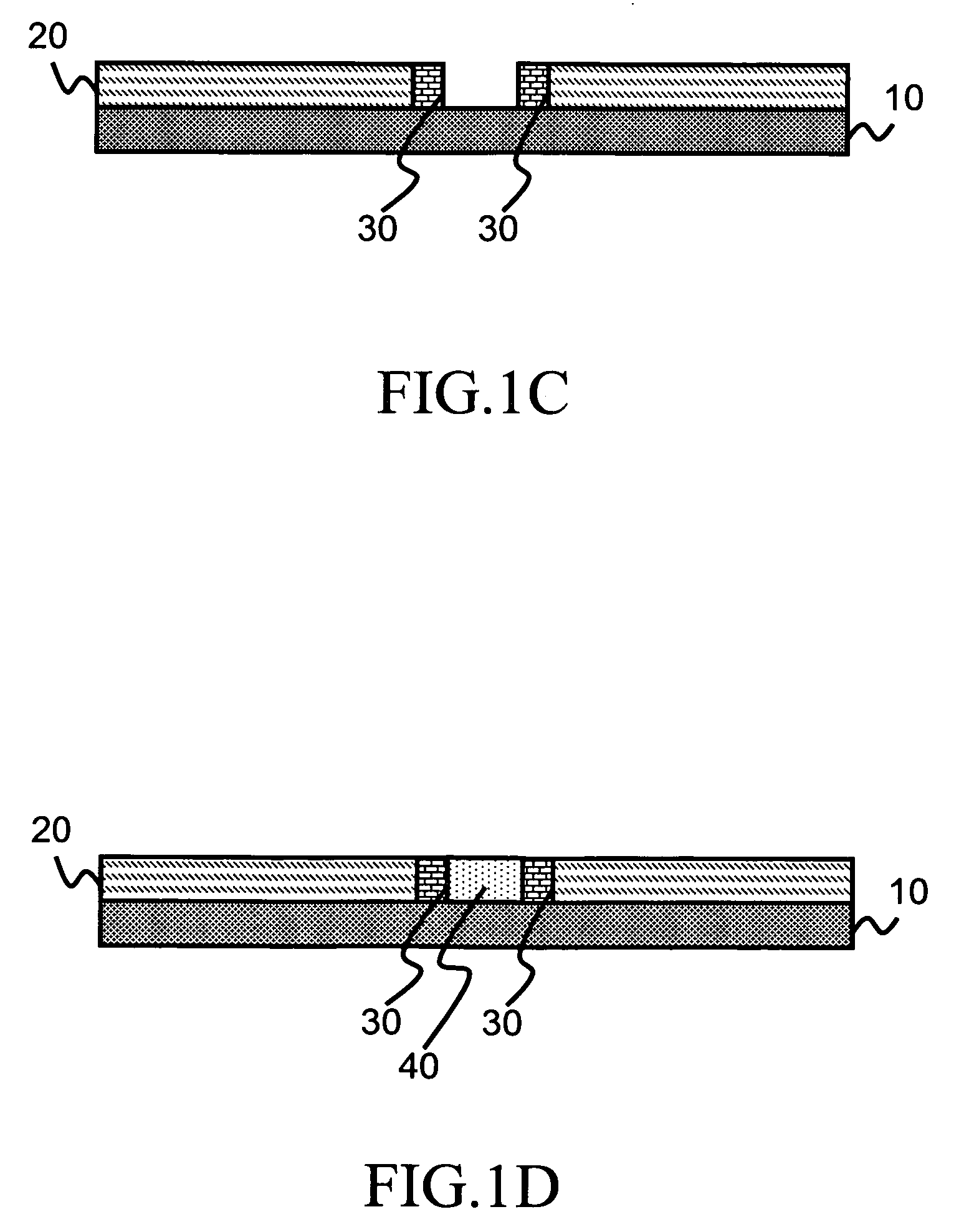
[0029] Referring to FIG. 1A, FIG. 1B, FIG. 1C, FIG. 1D, FIG. 1E, and FIG. 1F, they are cross-sectional views of a lateral phase change memory with spacer electrodes and method of manufacturing the same according to the present invention. First, a silicon oxide material is deposited through the conventional Chemical Vapor Deposition (CVD) or Physical Vapor Deposition (PVD) process to form a first insulating dielectric layer 10, as shown in FIG. 1A.

[0030] The above first insulating dielectric layer 10 can be formed by various dielectric materials, including silicon oxide materials, silicon nitride materials, low dielectric constant materials, and fluorine doped glass materials (e.g. fluorine doped glass (FSG)) formed through the process, such as plasma enhanced chemical vapor deposition (PECVD), plasma enhanced tetraethylorthosilicate (PETEOS), borophosphorus doped tetraethylorthosilicate (BPTEOS), boron doped tetraethylorthosilicate (BTEOS), phosphorous doped tetraethylorthosilicate ...

second embodiment

[0043] Referring to FIG. 2A, FIG. 2B, FIG. 2C, FIG. 2D, FIG. 2E, FIG. 2F, FIG. 2G, FIG. 2H, and FIG. 2I, they are cross-sectional views of a lateral phase change memory with spacer electrodes and method of manufacturing the same according to the present invention.

[0044] First, as shown in FIG. 2A, a semiconductor element 100 is formed through IC processing technique. The semiconductor element 100 can be a Metal Oxide Semiconductor Field Effect Transistor (MOSFET) with a gate, a source, and a drain, or a Bipolar Junction Transistor (BJT) with a base, a collector, and an emitter. The second embodiment is illustrated with the phase change memory of the present invention and the MOSFET on the same substrate.

[0045] As shown in FIG. 2B, a dielectric, such as, silicon oxide or silicon nitride is deposited on the MOSFET through the conventional CVD or PVD process, to form an insulating dielectric layer. After the insulating dielectric layer 80 is formed, it is patterned and etched to form ...


PUM


Abstract

A lateral phase change memory with spacer electrodes and method of manufacturing the same are provided. The memory is formed by connecting the conductive electrodes with lower resistivity and the spacer electrodes with higher resistivity, and filling the phase change material between the spacer electrodes. Therefore, the area that the phase change material contacts the spacer electrodes and the volume of the phase change material can be reduced; thereby the programming current and power consumption of the phase change memory are reduced.

Description

CROSS-REFERENCE TO RELATED APPLICATIONS [0001] This non-provisional application claims priority under 35 U.S.C. § 119(a) on Patent Application No. 094142136 filed in Taiwan, R.O.C. on Nov. 30, 2005, the entire contents of which are hereby incorporated by reference. BACKGROUND OF THE INVENTION [0002] 1. Field of Invention [0003] The present invention relates to a phase change memory, and more particularly to a lateral phase change memory with spacer electrodes and method of manufacturing the same, wherein the phase change memory has electrodes with a smaller contact area formed therein, so as to reduce the required programming current for the phase change. [0004] 2. Related Art [0005] Many different materials have two or more states, and materials with two states are particularly suitable for being used in digital memory. The state of the chalcogenide materials can be changed in a thermal inductive way as the temperature changes, so as to be in an amorphous state or a crystalline sta...

Claims


Application Information

Patent Timeline
Patent Type & Authority Applications(United States)
IPC IPC(8): H01L29/04
CPCH01L27/2436H01L45/06H01L45/1226H01L45/126H01L45/143H01L45/144H01L45/148H01L45/1683H10B63/30H10N70/823H10N70/8413H10N70/8825H10N70/884H10N70/231H10N70/066H10N70/8828
Inventor CHAO, TE-SHENGWANG, WEN-HANLEE, MIN-HUNGHSU, HONG-HUILEE, CHIEN-MINCHUO, YENCHEN, YI-CHANCHEN, WEI-SU
Owner IND TECH RES INST
Why Eureka
Try Eureka