[0012] A fuller understanding of the present invention and the features and benefits thereof will be accomplished upon review of the following detailed description together with the accompanying drawings, in which:
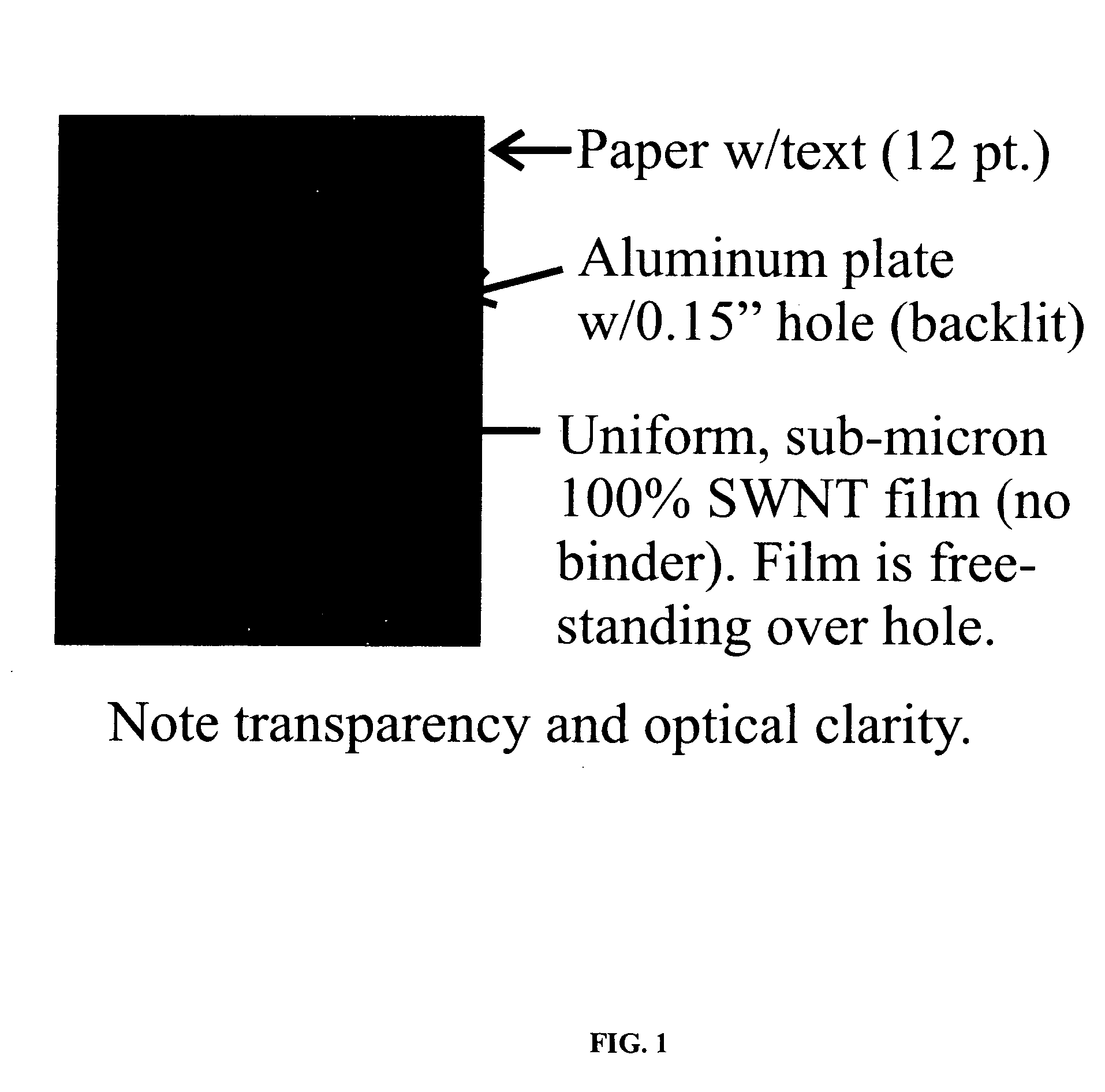
[0013]FIG. 1 illustrates a scanned image of a transparent 300 nm thick SWNT film stretched across a hole on an aluminum plate, the film formed according to a preferred method for forming films according to the invention.
[0014]FIG. 2 illustrates the transparency and
clarity of a thinner (about 90 nm), but larger
diameter film as compared to the film shown in FIG. 1 mounted on a plastic sheet.
[0015]FIG. 3 illustrates the transmission spectrum for a 50 nm SWNT film on a
quartz substrate and a 240 nm thick freestanding SWNT film formed according to an embodiment of the invention, for both doped and de-doped films, showing
high transmittance throughout the visible and the NIR range. The freestanding, thicker, film allowed recording of the
transmittance over the broad spectral range without interfering absorption from a supporting substrate.
[0017] Bulk electrical conductivity in
nanotube aggregates requires that some appreciable fraction of the nanotubes be electrically conducting and that this fraction have sufficient intimate electrical contact with each other to transport charge throughout the bulk. Electrical conductivity of the nanotubes themselves can come from two sources. A first source is from the
metallic nanotubes in the sample, which comprise about ⅓ of the nanotubes in SWNT material obtained commercially. A
second source can come from semiconducting nanotubes in the sample, provided the semiconducting nanotubes are doped with a suitable charge transfer species. For example, halogens such as
bromine and
iodine, or
alkali metal atoms, as well as certain other atoms or molecules, can be used as charge transfer species. Bulk electrical conductivity of the film is maximized by a high degree of nanotube contact, as well as the nanotube surfaces being largely free of any residual stabilizing agent since
stabilizing agents tend to be electrically insulating materials.
[0018] Films according to the present invention are generally essentially pure nanotube films, defined herein as films having at least 99% nanotubes by weight. However, the present invention includes nanotube composites, which can include a lower percentage of nanotubes, such as 80 or 90% by weight nanotubes, along with one or more generally
electrically conductive materials.
[0019] The film thickness can be tailored to range from a few tens of nanometers to several micrometers. The films produced using the invention have a substantially uniform nanotube density across their area which results in optical
clarity.
Optical transparency is enhanced for thin films(e.g. ≦100 nm) as compared to thicker films (e.g. 3 μm). Film thicknesses in the upper range generally become opaque. Particularly for transmission into the IR,
optical transparency is believed to be enhanced by a low nanotube carrier density.
[0020] A preferred method for forming electrically conductive and optical transparent SWNT films which exhibit uniform
optical density across their area includes the step of dispersing a low concentration of SWNTs, such as 0.005 mg / ml, in a solution, such as an
aqueous solution, containing a sufficient concentration of stabilizing agent to suspend the nanotubes. Commercially available single walled carbon nanotubes, such as from Carbon Nanotechnologies Incorporated, Houston, Tex. provide roughly ⅓
metallic nanotubes and ⅔ semiconducting nanotubes. Preferably, the nanotubes used are purified to remove the large catalyst particles which are utilized in their formation.
[0021] The stabilizing agent can comprise a variety of surfactants such as
sodium dodecyl sulfate (SDS) and TRITON X-100™, or surface stabilizing polymers. TRITON X-100™ is manufactured by the Dow Chemical Corporation, MI (formerly the Union
Carbide Corporation). TRITON X-100™ is octylphenol
ethylene oxide condensate and is also referred to as OCTOXYNOL-9™. This material has a molecular weight of 625 amu.
[0022] In this preferred method, the SWNT solution is then applied to a porous material. The porous material preferably comprises a filter membrane material, such as
polycarbonate or mixed
cellulose ester. The filter membrane preferably provides the following features:
[0024] 2) a high volume of
porosity with a plurality of sub-micron pores, and
[0025] 3) a composition that permits removal of the membrane material without disruption of the thin SWNT film, such as through
dissolution of the membrane material in a
solvent or
digestion of the membrane material in an acid.

