

Patterning method and methods for producing electro-optic device, color filter, illuminant, and thin-film tranisistor
a technology of tranisistor and electrooptic device, which is applied in the direction of photomechanical equipment, identification devices, instruments, etc., can solve the problems of reducing the range of choices in designing the manufacturing process, not forming a desired lyophilic pattern and lyophobic pattern,
- Summary
- Abstract
- Description
- Claims
- Application Information
AI Technical Summary
Benefits of technology
Problems solved by technology
Method used
Image

Examples
experimental example
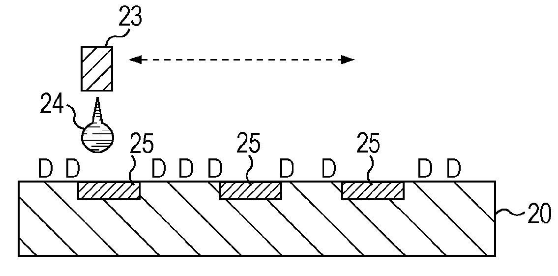
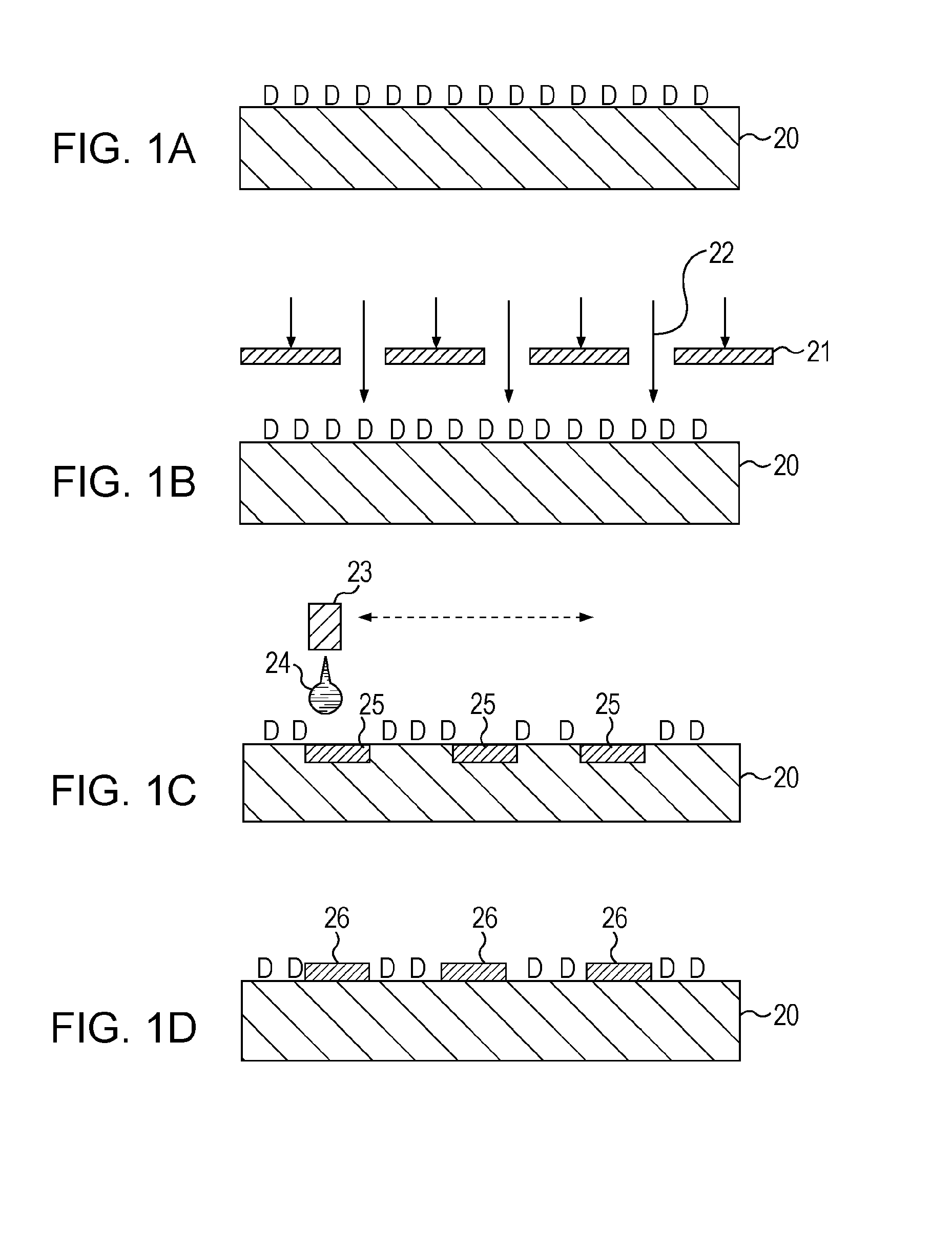
[0060]A test piece was first prepared as described below. An amorphous silicon oxide layer was formed to a thickness of 100 nm over the surface of a single crystal silicon substrate by thermal oxidation. Subsequently, an amorphous silicon (hereinafter referred to as “a-Si”) layer was formed to a thickness of 400 nm on the amorphous silicon oxide layer by CVD. Then, an amorphous silicon oxide layer was formed to a thickness of 50 nm on the a-Si layer by plasma CVD.
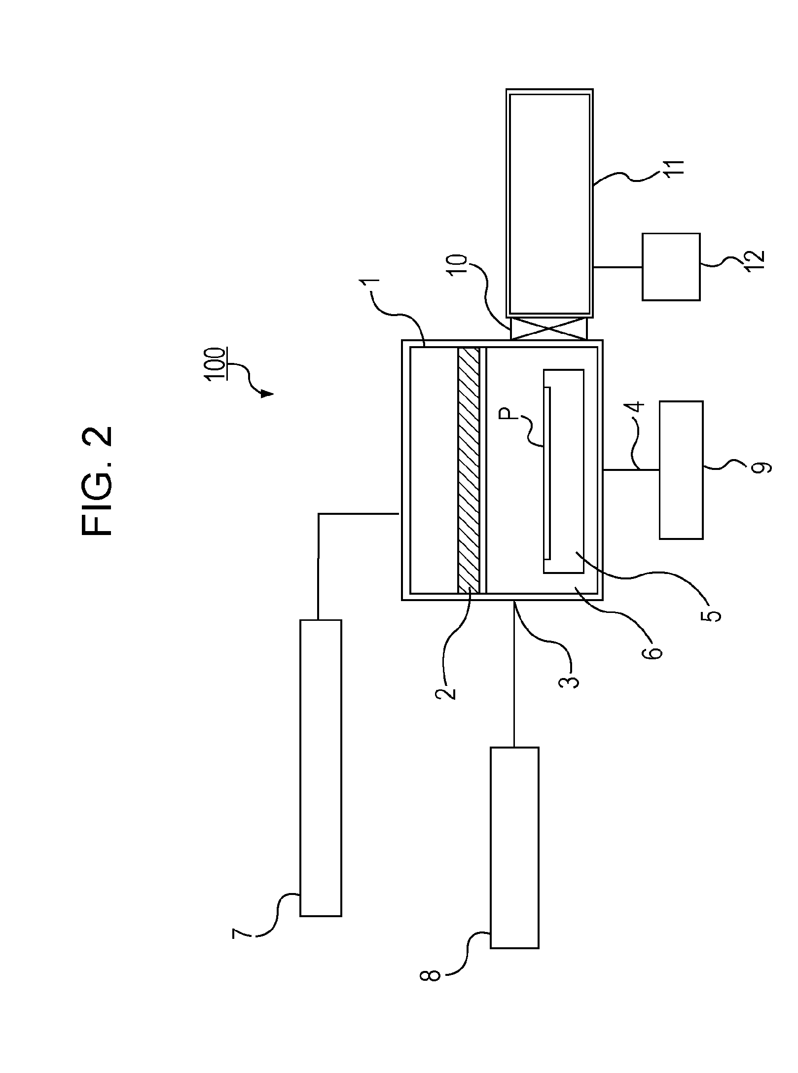
[0061]The resulting test piece was surface-treated in the apparatus 100 shown in FIG. 1.
[0062]The temperature of the heater stage 5 on which the test piece was placed was set at 280° C., and the internal pressure of the treatment chamber 6 was controlled to 66.7 Pa with the exhaust system while deuterium (D2) was being introduced as the treatment gas.
[0063]Microwaves of 2.45 GHz were generated from the microwave generator 7 at a power of 3 kW with the above conditions maintained. The microwaves were introduced into the trea...
first embodiment
[0088]A first embodiment illustrated in FIGS. 4A to 4C describes a method for producing an organic EL display device.
[0089]In the production of the organic EL display device, first, lower electrodes 51 made of, for example, aluminum, silver, ITO, or the like are formed on a substrate 50 by, for example, deposition and patterning, as shown in FIG. 4A. The lower electrodes 51 are covered with a layer of polyimide, silicon nitride, silicon oxide, or the like for forming element isolation regions. This layer is patterned so as to straddle each two adjacent lower electrodes 51 and then cleaned, thus forming the element isolation regions 52. Accordingly the element isolation regions 52 are disposed between two adjacent lower electrodes 51.
[0090]Then, plasma is generated in an atmosphere containing deuterium gas and hydrogen gas, and the surface of the substrate; that is, each surface of the lower electrodes 51 and element isolation regions 52, is exposed to the plasma for surface treatmen...
second embodiment
[0107]A second embodiment describes a method for producing surface-conduction electron-emitting elements.
[0108]As shown in FIG. 5A, a pair of electrodes 61 and 62 is formed of platinum or the like by sputtering and etching on, for example, a silicon or glass substrate 60 whose surface has been oxidized.
[0109]After cleaning the substrate, plasma is generated in an atmosphere containing deuterium gas and hydrogen gas, and the surface of the substrate; that is, each surface of the substrate 60 and the pair of electrodes 61 and 62, is exposed to the plasma for surface treatment in the apparatus as shown in FIG. 1. Thus, the water adsorbed on the surface is removed to form a hydrophobic surface.
[0110]The hydrophobic surface of the substrate is exposed to ultraviolet light with a wavelength of 365 nm generated from a mercury lamp through an exposure mask. The mask allows the light to selectively irradiate part of the electrodes 61 and 62 and gaps between the electrodes. Thus, exposed regi...
PUM
| Property | Measurement | Unit |
|---|---|---|
| temperature | aaaaa | aaaaa |
| temperature | aaaaa | aaaaa |
| pressure | aaaaa | aaaaa |
Abstract
Description
Claims
Application Information