Method and apparatus for manufacturing microstructure and device manufactured thereby

Inactive Publication Date: 2007-08-02
SEIKO EPSON CORP
View PDF6 Cites 57 Cited by
  • Summary
  • Abstract
  • Description
  • Claims
  • Application Information

AI Technical Summary

Benefits of technology

[0011]An advantage of the present invention is to provide a method and apparatus for manufacturing a microstructure, which allow formation of a desired micro-pattern with high throughput and high reproducibility on the surface or interior of a machined body.
[0012]It is another advantage of the invention to provide a device that is manufactured by said excellent method for manufacturing a microstructure.
[0013]A method for manufacturing a microstructure according to a first aspect of the invention includes: dividing an incident laser beam into a plurality of diffracted beams by means of a diffractive optical element; concentrating said divided plurality of diffracted beams into mutually parallel diffracted beams by means of a telecentric lens; causing said mutually parallel diffracted beams to enter perpendicularly to a collection of

Problems solved by technology

However, conventional machining methods use a single Bessel beam and hence go with low manufacturing throughput.
Therefore, they require a large amount of time (from several to several tens of days) when machining a large area.
Because of such low throughputs, appropriate use in laser machining applications has not been found for those methods and, thus, dissemination of the machining technique has been hampered.
However, it is difficult to

Method used


Image

  • Method and apparatus for manufacturing microstructure and device manufactured thereby
  • Method and apparatus for manufacturing microstructure and device manufactured thereby
  • Method and apparatus for manufacturing microstructure and device manufactured thereby

Examples


first embodiment

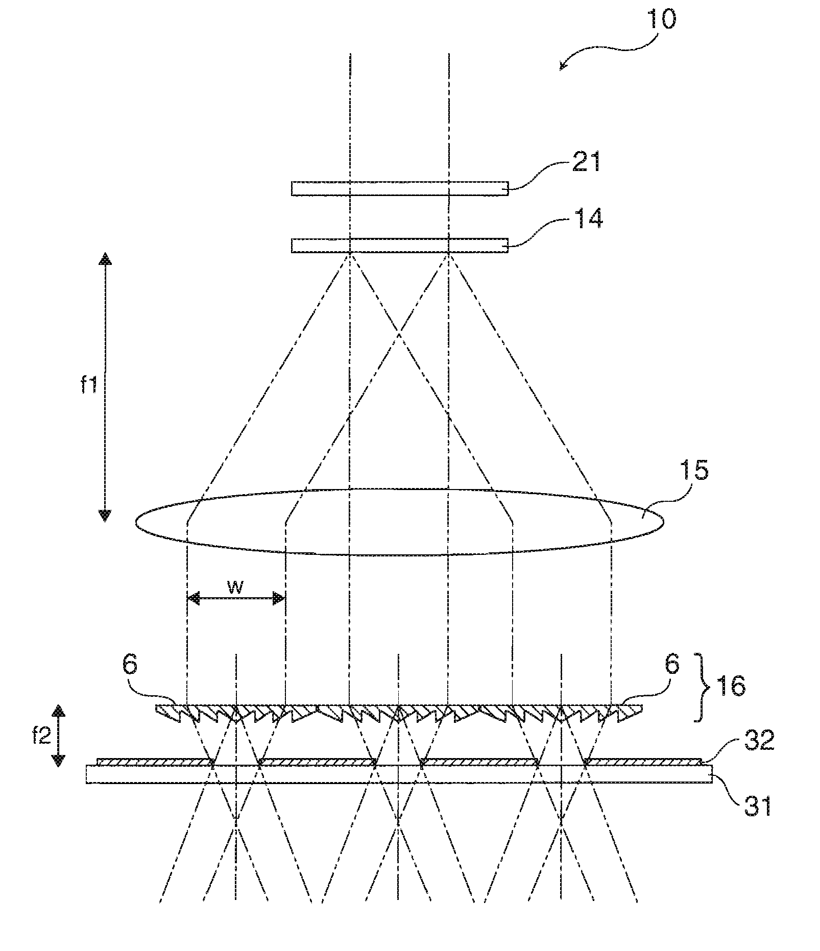
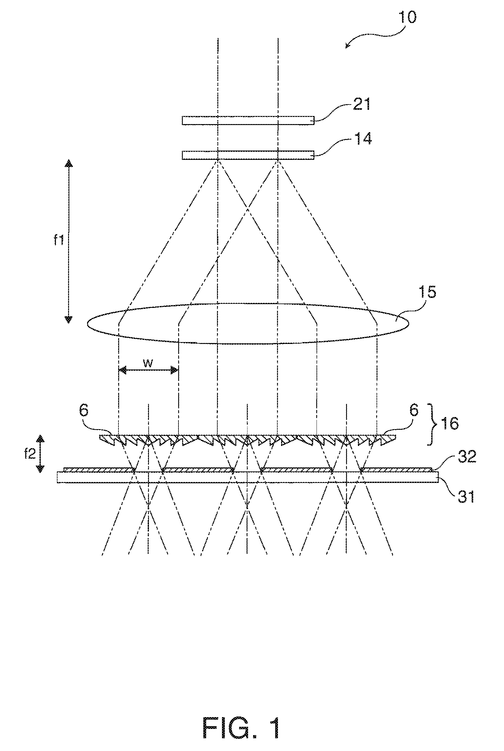
[0030]FIG. 1 diagrammatically shows an apparatus 10 for manufacturing a microstructure according to one embodiment of the invention.

[0031]As shown in FIG. 1, the apparatus 10 for manufacturing a microstructure includes: a quarter-wave plate 21; a diffractive optical element 14 that divides an incident laser beam into a plurality of diffracted beams; a telecentric lens 15 that concentrates the divided plurality of diffracted beams into mutually parallel diffracted beams; and a collection of axicons 16 that consists of a plurality of diffractive axicons 6 arranged into an array

[0032]In the present embodiment, a pulse laser with a pulse length of 10 nsec or less is used for the machining light source. For example, a Q-switch-oscillated Nd:YAG laser having a wavelength of 532 nm, an average power output of 1 W or less (at the pulse repetition of 1 kHz) and a beam diameter of 6 mm φ or less, is used.

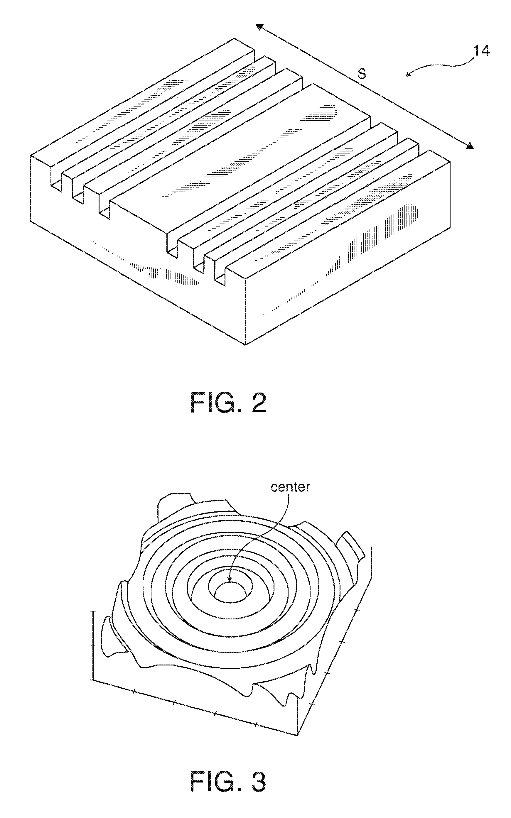
[0033]In FIG. 2, the relief structure of the diffractive optical element 14 employed in t...

second embodiment

[0040]As shown in FIG. 1, an incident laser beam is turned into a circularly-polarized light through the quarter-wave plate 21 to be divided into three diffracted beams having a mutually identical strength by the diffractive optical element 14.

[0041]Then, the divided three diffracted beams are focused as well as redirected by the telecentric lens 15 to turn into mutually parallel diffracted beams.

[0042]Furthermore, the three mutually parallel diffracted beams are caused to enter perpendicular to the complex of axicons 16, which is composed of three diffractive axicons 6 arranged in such a manner that the center of each diffracted beam and the center of each diffracting axicon 6 coincide, each beam being thereby diffracted by each diffractive axicon 6 to form three Bessel beams in line that propagate parallel in the same direction.

[0043]Then, by irradiating the generated three arrayed Bessel beams onto a machined body having a Cr film 32 formed on a glass substrate 31, for example, a...

first example

[0056]FIGS. 5A and 5B show an example of microholes machined by using the above method for manufacturing a microstructure. FIG. 5A is an SEM image of a microhole with a diameter of 2 μm or less, which has been manufactured by machining with a Bessel beam,. FIG. 5B is a graph showing the average size of a microholes manufactured with respect to different locations (vertical displacement) of a machining point. The machined body in the present embodiment is a Cr film 32 formed on a glass substrate 31, as in the case of the machined body shown in FIG. 1.

[0057]As shown in FIG. 5B, it has been found that the Bessel beam is able to drill microholes with a high reproducibility even if the machining point is vertically displaced by ±1 mm or more.


PUM

PropertyMeasurementUnit
Microstructureaaaaaaaaaa

Abstract

A method for manufacturing a microstructure, includes: dividing an incident laser beam into a plurality of diffracted beams by means of a diffractive optical element; concentrating said divided plurality of diffracted beams into mutually parallel diffracted beams by means of a telecentric lens; causing each of said mutually parallel diffracted beams to enter perpendicularly to the plane into a collection of axicons comprised of a plurality of axicons arranged into an array in such a manner that the center of each diffracted beam and the center of each axicon coincide, thereby forming a plurality of arrayed Bessel beams; and irradiating said plurality of arrayed Bessel beams onto a machined body.

Description

BACKGROUND OF THE INVENTION[0001]1. Technical field[0002]The present invention relates to a method and apparatus for manufacturing a microstructure and a device manufactured thereby. Specifically, the invention relates to a method and apparatus for manufacturing a microstructure, which allow formation of desired micro-patterns on the surface or interior of machined bodies with high throughput and high reproducibility. The invention also relates to a device manufactured thereby.[0003]2. Related Art[0004]A Bessel beam has a long focal depth and, therefore, if it is applied to laser machining, high reproducibility can be attained, even if the machining point is displaced in the depth direction due to such a condition that the machined surface is wavy and / or uneven in thickness. It also allows the interior of a thick transparent material to be machined by one operation. Thus, there is increasing interest in the laser micromachining technology using Bessel beams.[0005]Regarding micromach...

Claims


Application Information

Patent Timeline
IPC IPC(8): G03B27/42B23K26/00
CPCG03B21/625G03F7/70375
Inventor AMAKO, JUN
Owner SEIKO EPSON CORP
Why Eureka
Try Eureka