Epitaxial wafer and method for producing epitaxial wafers

a production method and technology for epitaxial wafers, applied in the direction of crystal growth process, polycrystalline material growth, protective fluid, etc., can solve the problems of aforementioned mirror wafer without epitaxial deposition, less ig ability of epitaxial wafers, and inability to induce oxygen precipitation in epitaxial wafers during device processing

Active Publication Date: 2007-08-02
SILTRONIC AG
View PDF49 Cites 13 Cited by
  • Summary
  • Abstract
  • Description
  • Claims
  • Application Information

AI Technical Summary

Benefits of technology

[0063] (1) An epitaxial wafer having a single crystal layer formed by epitaxial growth on a silicon single crystal substrate, the epitaxial wafer characterized by the fact that the epitaxial wafer in consequence of a heat treatment at 1000° C. for 16 hours generates radial direction oxygen precipitate at the minimum density of not less than 1×10⁹ pieces/cm3 and the radial distribution variation of oxygen precipitate density of not more than 0.5 and forms as epi-layer defects on the whole surface of the epitaxial wafer not more than 0.05 occurrences of N-SF/cm2 and not more than 0.05 occurrences of E-pit/cm2.
[0064] (2) A method for the production of an epitaxial wafer set forth in the foregoing item (1), characterized by causing silicon single crystal in the process of being produced by the Czochralski method to grow under the conditions having the V/G value [mm2/° C. min] between the upper limit of 1.4 exp(6.2×10⁻¹⁶×nitrogen concentration [atoms/cm3])×(V/G) crit and the lower limit of 1.0 exp(−7.1×10¹⁶×nitrogen concentration [atoms/cm3])×(V/G) crit (wherein V denotes pulling speed [mm/min]; G denotes average temperature gradient [° C./mm] from the melting point to 1350° C. in the direction of crystal growth axis; and (V/G) crit denotes the V/G value for silicon single crystal without nitrogen dopant that is contiguous to the boundary of one region, the one region denoting a region into which excess interstitial atoms are introduced from the solid-liquid interface during the growth of crystal) and having the cooling speed of not lower than 4° C./minute between 1100 and 1000° C., subjecting the grown silicon single crystal to simultaneous doping of nitrogen and carbon at a nitrogen concentration of 5×10¹⁴ to 5×10¹⁵ atoms/cm3 and a carbon concentration of 1×10¹⁶ to 1×10¹⁸ atoms/cm3 and using a base plate cut from the silicon single crystal resulting from the addition as a substrate, and depositing on the surface of the substrate a silicon single crystal layer by the epitaxial method.
[0065] (3) The I region mentioned above is characterized by being a region having a dislocation pit density of not less than 10 occurrences/cm2.
[0066] Here, the range of the nitrogen concentration and V/G is set between the upp

Problems solved by technology

The epitaxial wafer is typically produced by a process of epitaxial deposition that consists in depositing a silicon single crystal layer at a high temperature of at least 1100° C. Thus, the epitaxial wafer subjected to this high-temperature treatment is less capable of inducing oxygen precipitation during device processing and becomes inferior in the gettering property to the aforementioned mirror wafer that lacks epi-deposition.
The cause of this disadvantage is believed to be that the oxygen precipitation nuclei are diminished or eliminated during the high-temperature heat treatment of the epi-deposition process and therefore oxygen precipitation does not occur in the subsequent device processing.
Since this method entails addition to the number of steps of process, it may lead to the disadvantage of increasing the cost of production of the epitaxial wafer.
In the case of the epitaxial wafer resulting from subjecting a carbon-doped substrate to epi-deposition, oxygen precipitation does not occur at temperatures above 800° C., though it does occur in a temperature range falling short of 800° C. Device processing rarely involves a heat treatment below 800° C., and therefore, possibly reveals deficiency in the IG ability because of the failure to induce oxygen precipitation sufficiently.
It has been found, however, that when the nitrogen-doped base plate is subjected to epi-deposition, the resultant epi-layer suffers occurrence of such crystal defects as N-SF and E-pit.
Since an electrode including such occurrences of defects suffers deterioration of such electric properties as TDDB, a base plate in which such occurrences of defects are present cannot be used as a silicon semiconductor base plate for a high-quality device.
It suffers the presence of voids resulting from aggregation of such atomic vacancies.
When the nitrogen concentration is lowered as in the growth condition region 1, however, since the density of oxygen precipitation is degraded, the ability of gettering is deteriorated inevitably in s

Method used


Image

  • Epitaxial wafer and method for producing epitaxial wafers
  • Epitaxial wafer and method for producing epitaxial wafers
  • Epitaxial wafer and method for producing epitaxial wafers

Examples


Embodiment Construction

[0136] Now, examples of this disclosure will be explained below.

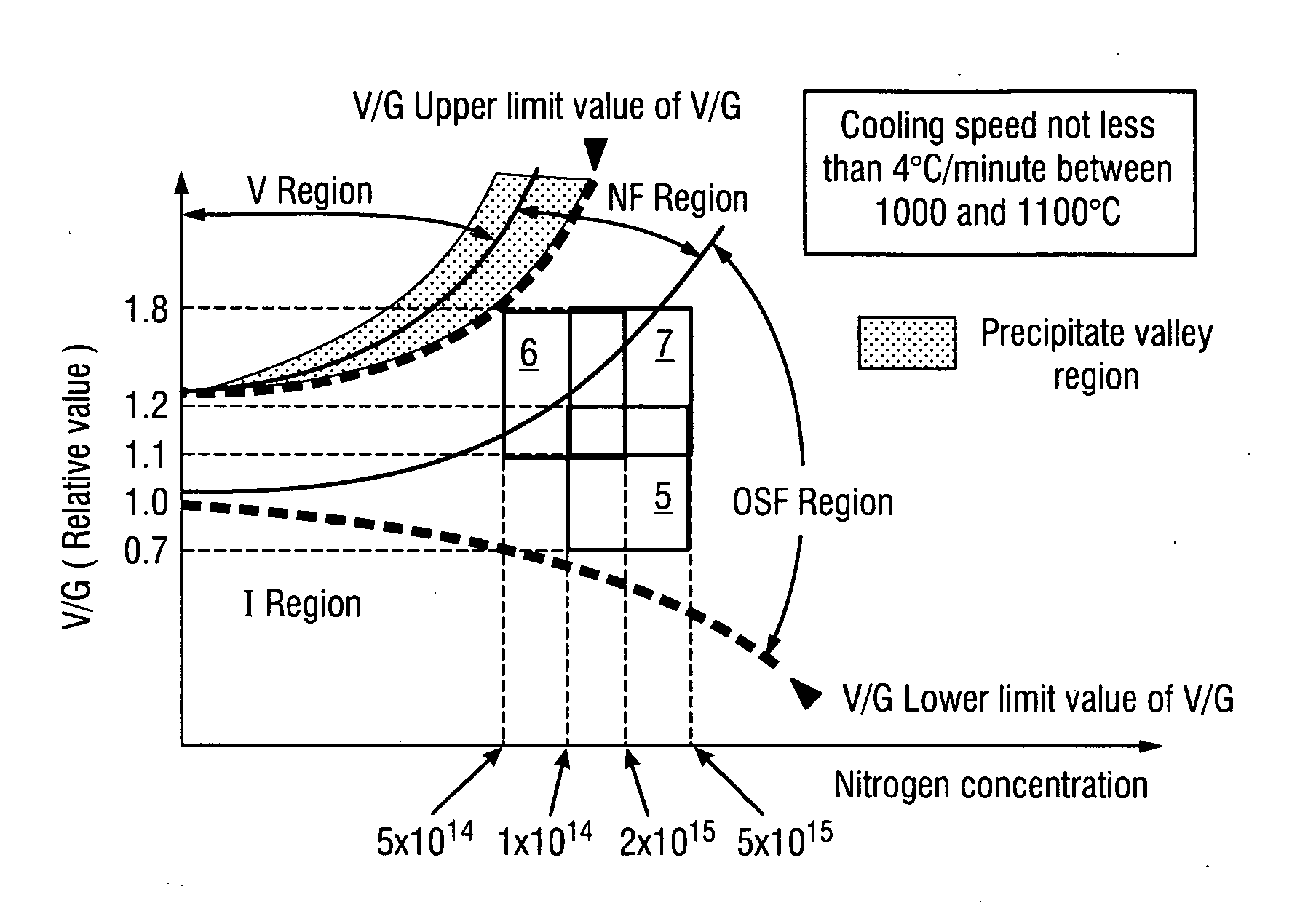
[0137] In the examples, the device for producing silicon single crystal is adapted to produce the silicon single crystal by the ordinary CZ method, and consists of the first pulling oven capable of typical pulling speeds and the second pulling oven adapted for additional cooling by a thermal shield plate for the purpose of heightening the cooling speed between 1100 and 1000° C. In embodying this disclosure, these pulling ovens do not need to be particularly limited to the examples herein but were only required to be capable of fulfilling the conditions of growth contemplated by this disclosure.

[0138] The silicon single crystal grown by the use of this device was a conduction type: p type (boron-doped) and crystal diameter of 8 inches (200 mm).

[0139] The addition of nitrogen was implemented by adding a base plate having a nitride film adhering thereto into a silicon melt. The addition of carbon was accomplished by add...


PUM


Abstract

This disclosure is aimed at providing a method for producing an epitaxial wafer allowing uniform occurrence of oxygen precipitate in a substrate plane in the radial direction in a base plate and excelling in the crystal quality of an epi-layer.
A method for the production of an epitaxial wafer, characterized by using as a substrate a base plate of nitrogen- and carbon-added silicon single crystal having a nitrogen concentration of 5×10¹⁴ to 5×10¹⁵ atoms/cm3 and a carbon concentration of 1×10¹⁶ to 1×10¹⁸ atoms/cm3, having a crystal growth condition during the production of silicon single crystal in a range in which the whole surface of substrate becomes an OSF region, and being pulled at a cooling speed of not less than 4° C./minute between 1100 and 1000° C. during the growth of crystal, and depositing the silicon single crystal layer on the surface of the substrate by the epitaxial method.

Description

RELATED APPLICATIONS [0001] The present application claims the benefit of Japanese Patent Application, Serial No. 2006-005237, filed on Jan. 12, 2006, the complete disclosure of which is hereby incorporated by reference herein in its entirety and for all purposes. The present application is also a Continuation-in-Part of U.S. Utility patent application Ser. No. 11 / 645,017, filed on Dec. 22, 2006, titled ANNEALED WAFER AND MANUFACTURING METHOD OF ANNEALED WAFER, the complete disclosure of which is hereby incorporated by reference herein in its entirety and for all purposes.FIELD OF THE DISCLOSURE [0002] This disclosure relates to an epitaxial wafer and a method for the production of an epitaxial wafer. BACKGROUND OF THE DISCLOSURE [0003] A semiconductor substrate, particularly a silicon single crystal wafer (hereinafter referred to occasionally as a “substrate”), is used as the substrate for the manufacture of a highly integrated MOS device. Most silicon single crystal wafers are sub...

Claims


Application Information

Patent Timeline
IPC IPC(8): H01L21/322
CPCC30B29/06C30B15/00H01L21/20
Inventor NAKAI, KATSUHIKOFUKUHARA, KOJI
Owner SILTRONIC AG
Why Eureka
Try Eureka