Method of forming deposited film and method of forming photovoltaic element

a technology of photovoltaic elements and deposited films, which is applied in the direction of solid-state diffusion coatings, plasma techniques, coatings, etc., can solve the problems of large number of experiments, small open-circuit voltage values, and difficult to solve, so as to reduce the number of experiments, and improve the conversion efficiency

Inactive Publication Date: 2007-08-09
CANON KK
View PDF2 Cites 17 Cited by
  • Summary
  • Abstract
  • Description
  • Claims
  • Application Information

AI Technical Summary

Benefits of technology

[0022]It is, therefore, an object of the present invention to provide a method of forming a deposited film which can optimize the conditions for forming a deposited film to strike a balance between the improvement in the conversion eff...

Problems solved by technology

However, in order to attain more excellent characteristics and further reduction of costs of the above-mentioned photovoltaic element or the like, there are still various problems to be solved.
However, it has been found that a larger short circuit current value tends to make the open circuit voltage value smaller.
Therefore, to find the well-balanced optimum conditions for forming the deposited film which is improved in both the short circuit current value and the open circuit voltage value at the same time, a lot of experiments are necessary, and adjustment of the conditions is extremely difficult.
In a deposited film containing microcrystalline silicon, there is a problem that, when the crystal grain diameter is small, or when there are many defects in the crystal boundaries, it is impossible to attain an open circuit voltage value which is large enough for a solar cell, and the short circuit current value is small.
In addition, there is also a problem that the film quality is degraded and the electrical characteristics and the like are lowered with the elapse of time.
Depending on the thickness of the deposited film, in the case of light irradiation for a long period of time, weak bonds of those bonds constituting a network are broken and the number of dangling bonds increases, which has an adverse effect on the characteristics.
Although those characteristics change depending on the conditions for forming the deposited film, the correlation between the conditions for forming the deposited film and the above-mentioned...

Method used


Image

  • Method of forming deposited film and method of forming photovoltaic element
  • Method of forming deposited film and method of forming photovoltaic element
  • Method of forming deposited film and method of forming photovoltaic element

Examples


example 1

[0181]A belt-shaped base member (40 cm in width, 200 m in length, and 0.125 mm in thickness) made of stainless steel (SUS430BA) was sufficiently degreased and cleaned, and then mounted to a continuous sputtering apparatus (not shown). An Ag thin film was vapor deposited in a thickness of 100 nm by sputtering using an Ag electrode as a target. Further, a ZnO thin film was vapor deposited in a thickness of 1.2 μm on the Ag thin film by sputtering using a ZnO target to thereby form a belt-shaped conductive substrate 501.

[0182]Then, the apparatus of the structure illustrated in FIG. 5 was used to deposit an n-type semiconductor layer, an i-type semiconductor layer, and a p-type semiconductor layer in sequence from the substrate side according to the above-mentioned procedure under the conditions in Table 1 with the pressure and the interelectrode distance during formation of the i-type layer being changed. After that, using a sputtering apparatus and a vapor deposition apparatus (not sh...

example 2

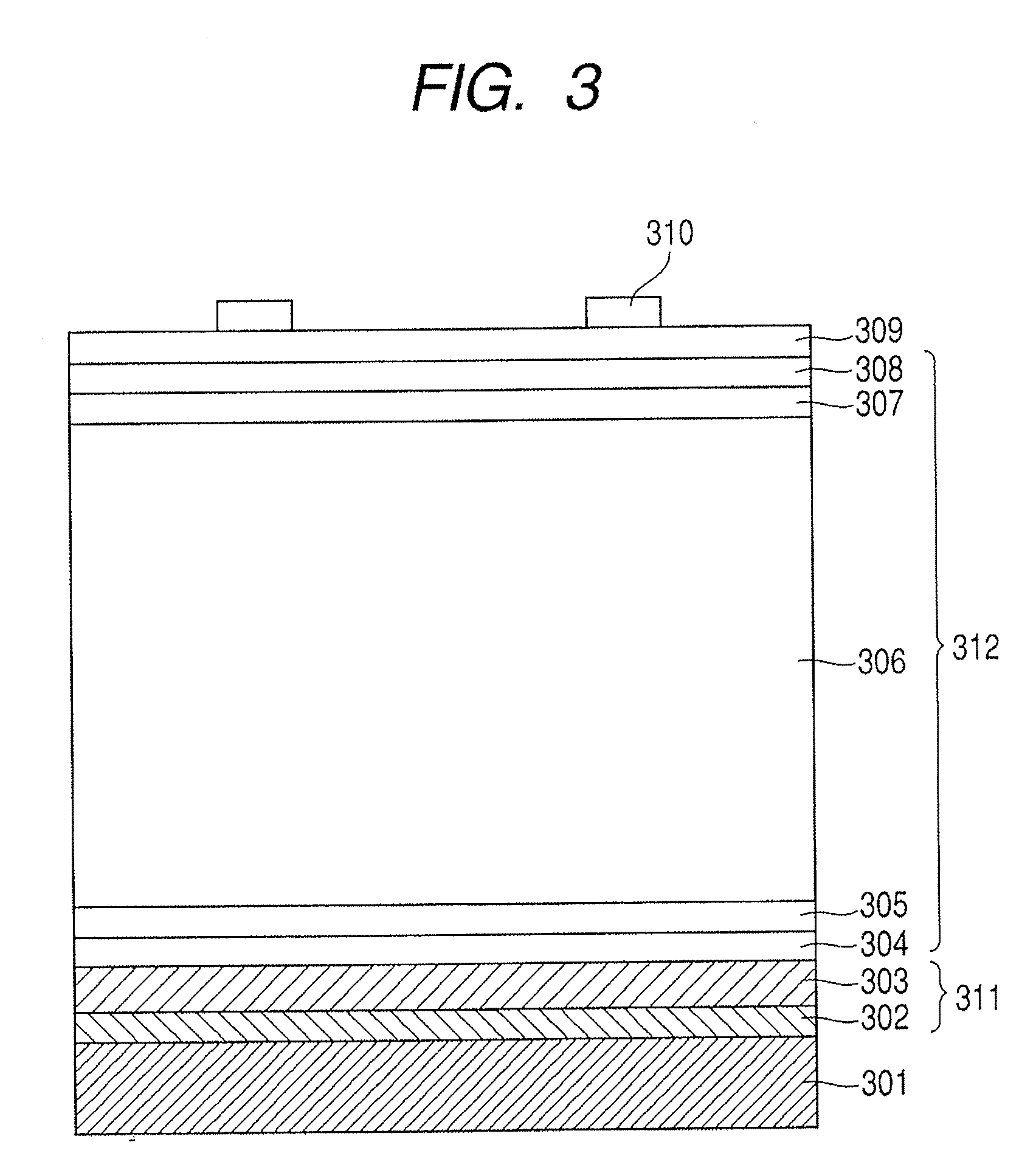
[0210]Samples of a solar cell (single cell) having a pin structure such as illustrated in FIG. 3 were made by following the same procedure as in Example 1 with the exception that the substrate temperature when the i-type layer was formed was changed as shown in the following Table 3.

TABLE 3n / ip / in-typebufferi-typebufferp-typelayerlayerlayerlayerlayerGas speciesand flow rateSiH4 (sccm)30155005050SiF4 (sccm)200H2 (slm)3.64100.415PH3 (%)5BF3 (%)30Bias voltage00−6000(V)Substrate temperature220250100 to220150(° C.)350Pressure10001000100010001000(Pa)High frequency power0.21.250.21.5(kW)(RF)(VHF)(VHF)(RF)(RF)Interelectrode distance101571510(mm)Film thickness2010200 / 1500105(nm)

[0211]The results are shown in Table 4 below. Incidentally, the item “region” in the characteristics of Table 4 is intended to mean classification of “amorphous region”, “microcrystalline region”, and “polysilane region” according to the results of the SEM observation and the RAMAN measurement of the formed samples.

TA...

example 3

[0216]Samples of a solar cell (single cell) having a pin structure such as illustrated in FIG. 3 were made by following the same procedure as in Example 1 with the exception that the bias voltage with respect to the interelectrode distance when the i-type layer was formed was changed as shown in Table 5 below.

TABLE 5n / ip / in-typebufferi-typebufferp-typelayerlayerlayerlayerlayerGas speciesand flow rateSiH4 (sccm)30155005050SiF4 (sccm)200H2 (slm)3.64100.415PH3 (%)5BF3 (%)30Bias voltage000 to00(V / cm)−400Substrate temperature220250190220150(° C.)Pressure10001000100010001000(Pa)High frequency power0.21.250.21.5(kW)(RF)(VHF)(VHF)(RF)(RF)Interelectrode101571510distance(mm)Film thickness (nm)2010200 / 1500105

[0217]The results are shown in Table 6 below. Incidentally, the item “region” in the characteristics of Table 6 is intended to mean classification of “amorphous region”, “microcrystalline region”, and “polysilane region” according to the results of the SEM observation and the RAMAN measure...


PUM

PropertyMeasurementUnit
Fractionaaaaaaaaaa
Temperatureaaaaaaaaaa

Abstract

Provided is a deposited film containing microcrystalline silicon by plasma CVD, which includes changing at least one of conditions selected from a high frequency power density, a bias voltage with respect to an interelectrode distance, a bias current with respect to an electrode area, a high frequency power with respect to a source gas flow rate, a ratio of a diluting gas flow rate to a source gas flow rate, a substrate temperature, a pressure, and an interelectrode distance, between conditions for forming a deposited film of a microcrystalline region and conditions for forming a deposited film of an amorphous region; and forming a deposited film under conditions within a predetermined range in the vicinity of boundary conditions under which the crystal system of the deposited film substantially changes between a amorphous state and a microcrystalline state.

Description

BACKGROUND OF THE INVENTION[0001]1. Field of the Invention[0002]The present invention relates to a method of forming a deposited film, and more particularly, to a silicon-based deposited film, and a method of forming a photovoltaic element using a silicon-based deposited film such as a solar cell.[0003]2. Description of the Related Art[0004]High frequency plasma CVD is an excellent method of mass-producing a silicon-based deposited film because a large area film can be formed easily at a low temperature and the process throughput is improved. A solar cell which is an application of a silicon-based deposited film to a product has an advantage in that the energy source is unlimited and the power generation process is clean as compared with a case of existing energy utilizing fossil fuel. However, in order to make a solar cell widely available, further reduction of costs is necessary. In attaining this, one important technical problem to be solved is to improve the film forming rate by...

Claims


Application Information

Patent Timeline
IPC IPC(8): C23C16/00
CPCC23C16/24C23C16/45523Y02E10/548Y02E10/545C23C16/545
Inventor TAKAI, YASUYOSHISANO, MASAFUMISAITO, KEISHI
Owner CANON KK
Why Eureka
Try Eureka