Method for manufacturing semiconductor device, substrate treater, and substrate treatment system
- Summary
- Abstract
- Description
- Claims
- Application Information
AI Technical Summary
Benefits of technology
Problems solved by technology
Method used
Image

Examples
first embodiment
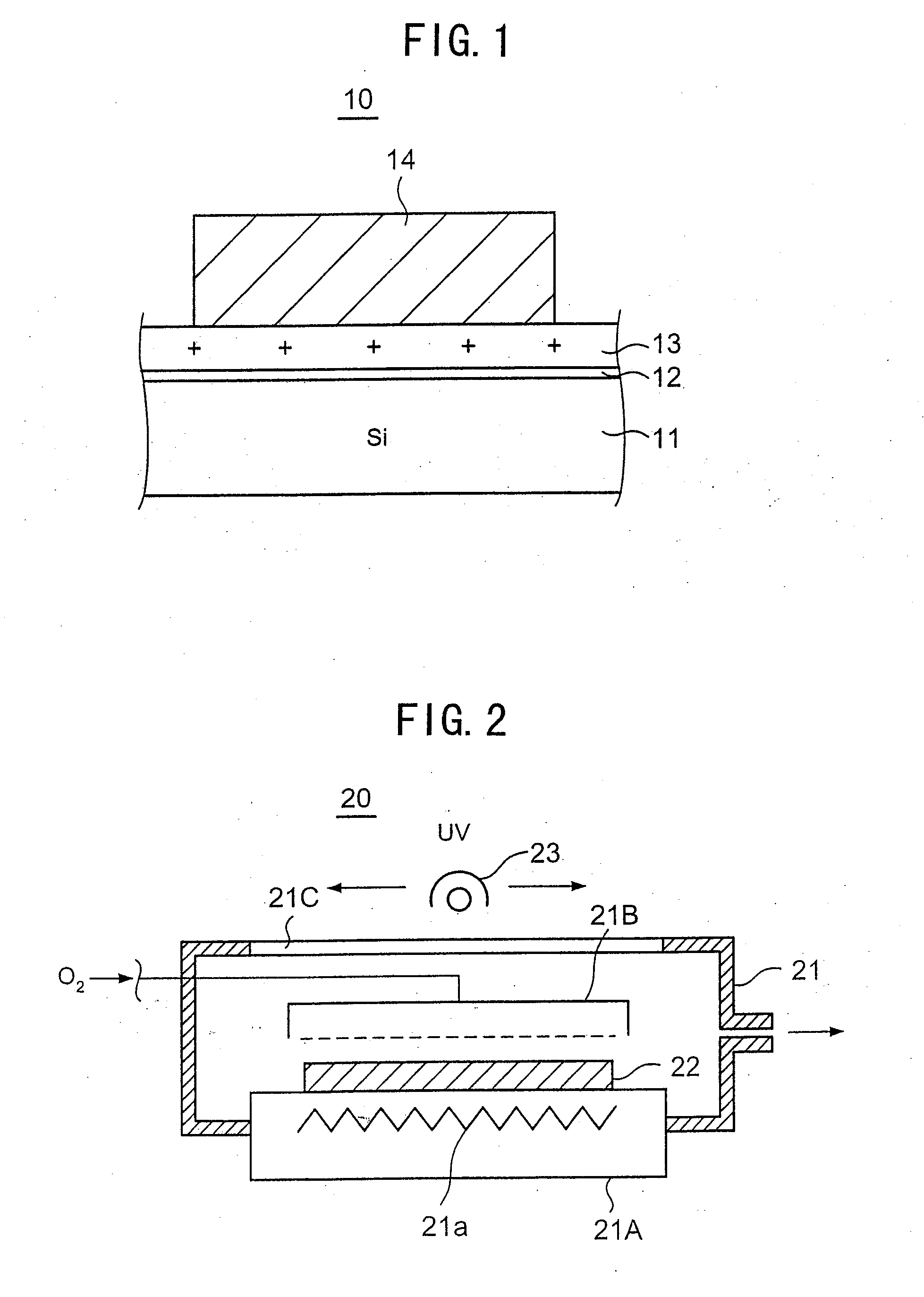
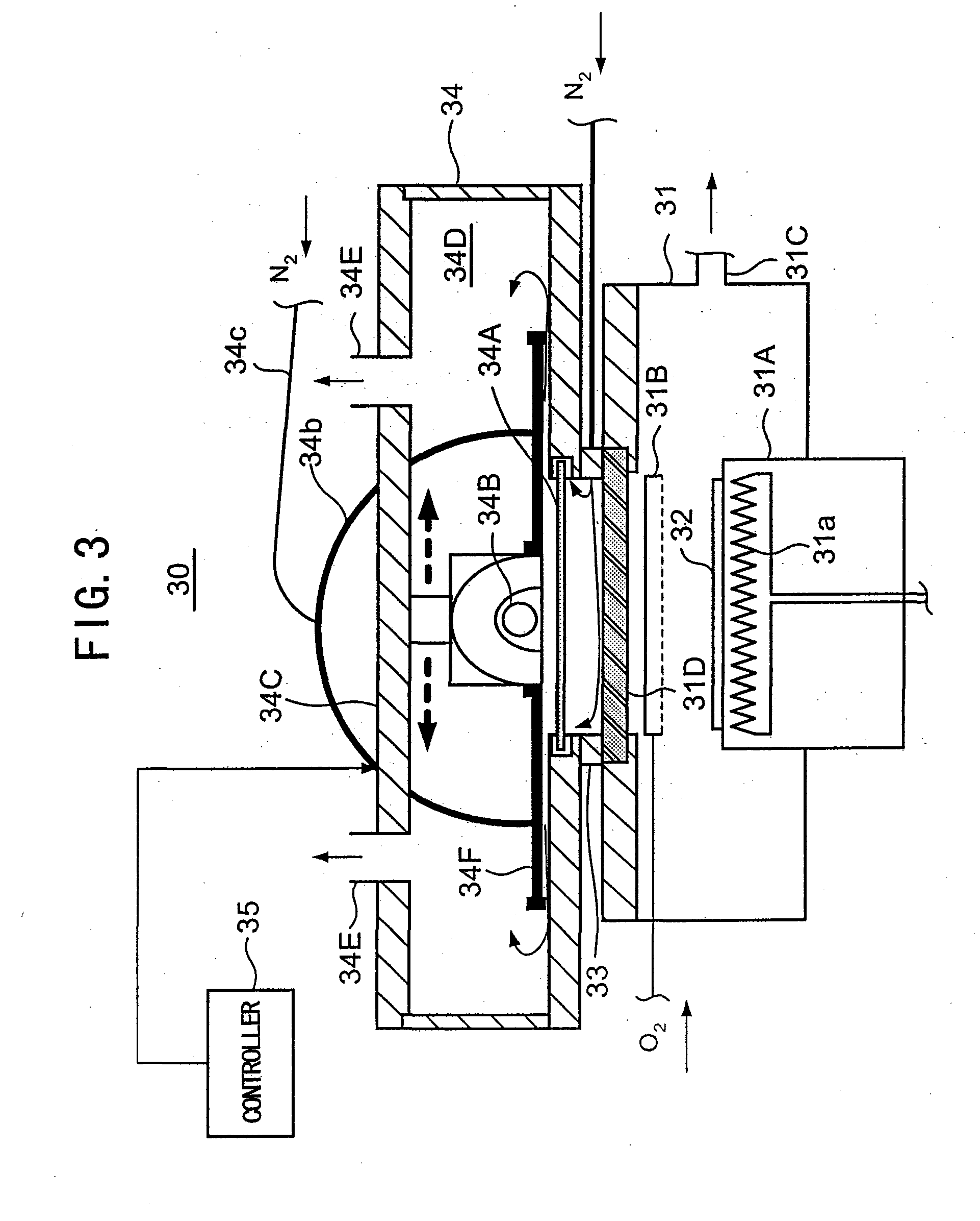
[0124]FIG. 3 shows the construction of the substrate processing apparatus 30 according to a first embodiment of the present invention.
[0125] Referring to FIG. 3, the substrate processing apparatus 13 includes a processing vessel 31 having a stage 31A holding substrate 32 to be processed thereon, and there is provided a showerhead 31B of a material such as quartz transparent to ultraviolet radiation. The showerhead 31B is provided so as to face the substrate on the stage 31A. Further, the processing vessel 31B is evacuated through an evacuation port 31C, and an oxidizing gas such as 02 is supplied to the foregoing showerhead 31B from an external gas source.
[0126] It should be noted that the processing vessel 31 is formed with an optical window 31B of a material transparent to ultraviolet radiation such as quartz above the showerhead 31B such that the optical window 31B exposes the showerhead 31B and the substrate 32 underneath the showerhead 31B. Further, the stage 31A is provided ...
second embodiment
[0159]FIG. 11 shows the construction of a substrate processing system 40 according to a second embodiment of the present invention in which the substrate processing apparatus 30 of FIG. 3 is incorporated.
[0160] Referring to FIG. 11, the substrate processing system 40 is a cluster type apparatus and includes a load lock chamber 41 used for loading and unloading a substrate, a preprocessing chamber 42 for processing the substrate surface by nitrogen radicals N* and hydrogen radicals H* and an NF3 gas. The preprocessing chamber thereby removes the native oxide film on the substrate surface by converting the same to an volatile film of N-0-Si—H system. Further, the cluster type processing apparatus includes a UV—O2 processing chamber 43 including the substrate processing apparatus 30 of FIG. 3, a CVD processing chamber 44 for depositing a high K dielectric film such as Ta205, Al2O3, ZrO2, HfO2, ZrSiO4, HfSiO4, and the like, and a cooling chamber 45 for cooling the substrate, wherein th...
third embodiment
[0164]FIG. 12 shows the construction of a substrate processing system 40A according to a third embodiment of the present invention.
[0165] Referring to FIG. 12, the substrate processing system 40A has the construction similar to that of the substrate processing system 40 except that there is provided a plasma nitridation processing chamber 44A in place of the CVD processing chamber 44.
[0166] The Plasma Nitridation Processing Chamber 44A is supplied with the substrate formed with the SiO2 film in the UV—O2 processing chamber 43 along a path (3), and a SiON film is formed on the surface thereof by plasma nitridation processing.
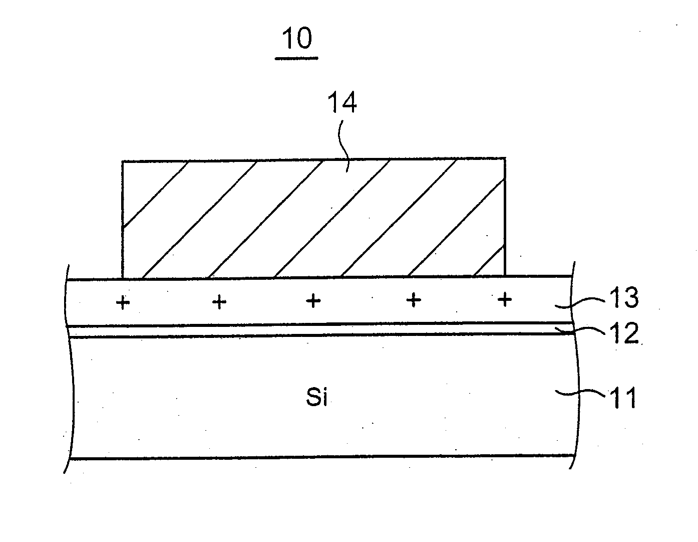
[0167] By repeating such process steps between the UV—O2 processing chamber 43 and the plasma nitridation processing chamber 44A, a semiconductor device 10A having a SiON gate insulation film 13A shown in FIG. 13 is obtained. In FIG. 13, it should be noted that those parts explained previously are designated by the same reference numerals and the description t...
PUM
| Property | Measurement | Unit |
|---|---|---|
| Thickness | aaaaa | aaaaa |
| Thickness | aaaaa | aaaaa |
| Thickness | aaaaa | aaaaa |
Abstract
Description
Claims
Application Information
 - R&D
- Intellectual Property
- Life Sciences
- Materials
- Tech Scout
- Unparalleled Data Quality
- Higher Quality Content
- 60% Fewer Hallucinations
Browse by: Latest US Patents, China's latest patents, Technical Efficacy Thesaurus, Application Domain, Technology Topic, Popular Technical Reports.
© 2025 PatSnap. All rights reserved.Legal|Privacy policy|Modern Slavery Act Transparency Statement|Sitemap|About US| Contact US: help@patsnap.com