Silicon single crystal wafer for IGBT and method for manufacturing silicon single crystal wafer for IGBT

Active Publication Date: 2007-08-23
SUMCO CORP
View PDF63 Cites 46 Cited by
  • Summary
  • Abstract
  • Description
  • Claims
  • Application Information

AI Technical Summary

Benefits of technology

[0057]According to the method for manufacturing a silicon single crystal wafer for IGBT as described above, the tolerance of the rate that allows silicon single crystals to be pulled that are free of grown-in defects can be increased by introducing a hydrogen atom-containing substance within a hydrogen gas equivalent partial pressure of 40 to 400 Pa, and as a result, wafers can be easily produced from which COP defects and dislocation clusters are eliminated throughout the entire region in the radial direction of the crystal. In addition, by either doping irradiating non-doped silicon single crystals with neutrons and doping with phosphorous after pulling, or adding an n-type dopant such as phosphorous to the silicon melt, variation in resistivity within the crystal surface can be made to

Problems solved by technology

When silicon single crystal wafers are produced according to the Czochralski method (CZ method), although it is possible to produce large-diameter wafers having a diameter of about 300 mm, wafers produced using the CZ method were not suitable for wafers for IGBT for the reasons indicated below.
During production of IGBT, a gate oxide film is formed on the wafer surface,

Method used


Image

  • Silicon single crystal wafer for IGBT and method for manufacturing silicon single crystal wafer for IGBT
  • Silicon single crystal wafer for IGBT and method for manufacturing silicon single crystal wafer for IGBT
  • Silicon single crystal wafer for IGBT and method for manufacturing silicon single crystal wafer for IGBT

Examples


Example

Experimental Example 1

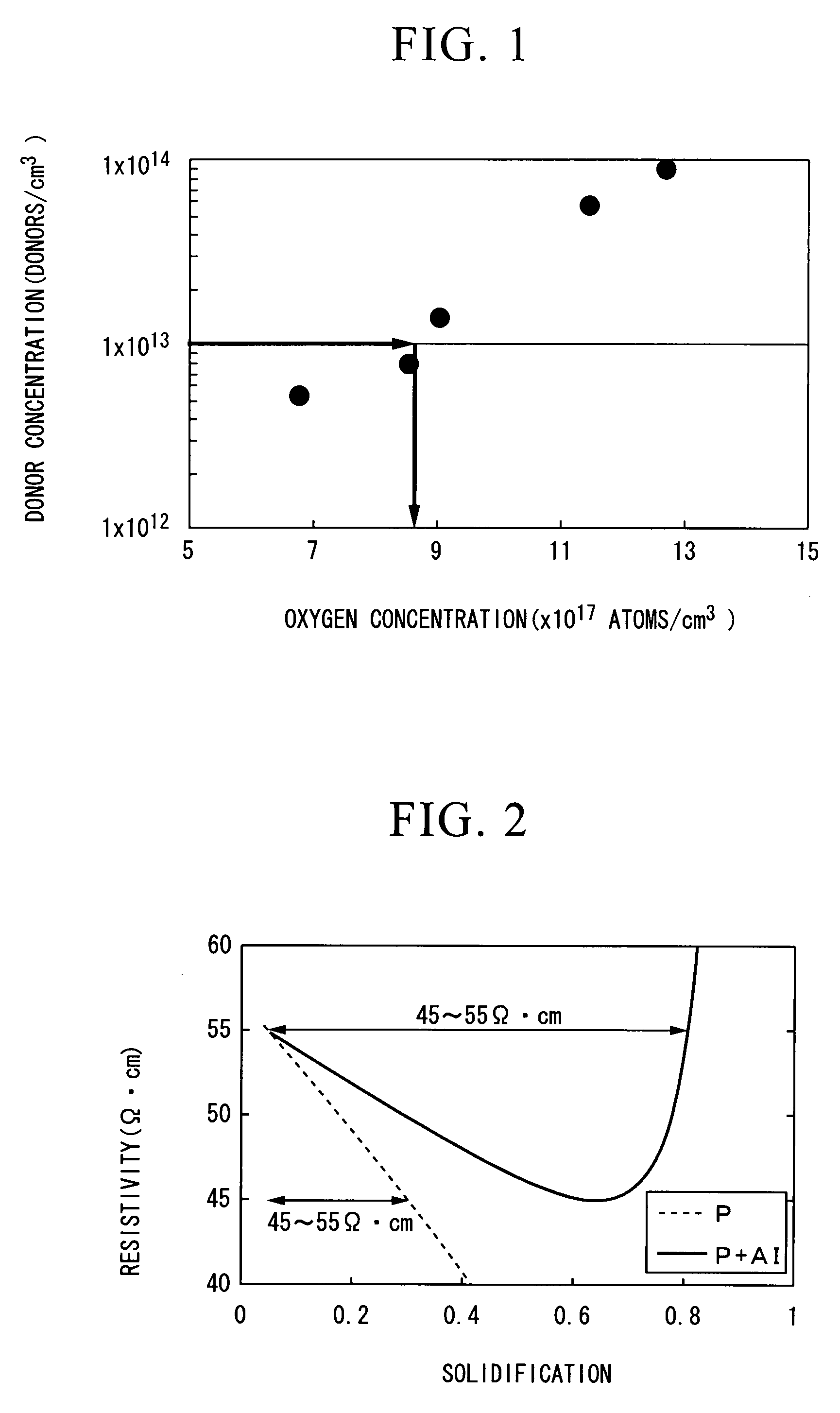
[0102]Silicon ingots having various interstitial oxygen concentrations were produced by the CZ method. More specifically, polycrystalline silicon chunks were placed in a quartz crucible and then the polycrystalline silicon chunks are heated in an argon atmosphere to obtain a silicon melt. Phosphorous as a dopant was added to this silicon melt. The amount of phosphorous added was adjusted such that the resistivity of the silicon single crystal was 65 Ω·cm. Next, a seed crystal was immersed in the silicon melt while supplying a horizontal magnetic field of 3000 G (0.3 T) from a magnetic field generator such that the height of the center of the magnetic field was −75 to +50 mm from the surface of the silicone melt, after which the seed crystal and the quartz crucible were rotated while growing single crystals from the bottom of the seed crystal by gradually pulling the seed crystal. Furthermore, the ratio V / G, wherein the single crystal growth rate (pulling speed)...

Example

Experimental Example 2

[0110]Silicon ingots having various interstitial oxygen concentrations were produced by the CZ method. More specifically, polycrystalline silicon chunks were placed in a quartz crucible and then the polycrystalline silicon chunks are heated in an argon atmosphere to obtain a silicon melt. Next, a seed crystal was immersed in the silicon melt while supplying a horizontal magnetic field of 3000 G (0.3 T) from a magnetic field generator such that the height of the center of the magnetic field was −75 to +50 mm from the surface of the silicone melt, after which the seed crystal and quartz crucible were rotated while growing single crystals from the bottom of the seed crystal by gradually pulling the seed crystal. Furthermore, the ratio V / G, wherein the single crystal growth rate (pulling speed) is defined as V (mm / min) and the temperature gradient from the melting point to 1350° C. during single crystal growth is defined as G (° C. / mm), was set to about 0.185, and ...


PUM


Abstract

In this silicon single crystal wafer for IGBT, COP defects and dislocation clusters are eliminated from the entire region in the radial direction of the crystal, the interstitial oxygen concentration is 8.5×10¹⁷ atoms/cm3 or less, and variation in resistivity within the wafer surface is 5% or less. This method for manufacturing a silicon single crystal wafer for IGBT includes introducing a hydrogen atom-containing substance into an atmospheric gas at a hydrogen gas equivalent partial pressure of 40 to 400 Pa, and growing a single crystal having an interstitial oxygen concentration of 8.5×10¹⁷ atoms/cm3 or less at a silicon single crystal pulling speed enabling pulling of a silicon single crystal free of grown-in defects. The pulled silicon single crystal is irradiated with neutrons so as to dope with phosphorous; or an n-type dopant is added to the silicon melt; or phosphorous is added to the silicon melt so that the phosphorous concentration in the silicon single crystal is 2.9×10¹³ to 2.9×10¹⁵ atoms/cm3 and a p-type dopant having a segregation coefficient smaller than that of the phosphorous is added to the silicon melt so that the concentration in the silicon single crystals is 1×10¹³ to 1×10¹⁵ atoms/cm3 corresponding to the segregation coefficient thereof.

Description

BACKGROUND OF THE INVENTION[0001]1. Field of the Invention[0002]The present invention relates to a silicon single crystal wafer for IGBT used in the production of insulated gate bipolar transistors (IGBT), and a method for manufacturing a silicon single crystal wafer for IGBT.[0003]The present application claims priority from Japanese Patent Application No. 2006-043572, filed on Feb. 21, 2006 and Japanese Patent Application No. 2007-034536, filed on Feb. 15, 2007, the contents of which are incorporated herein by reference.[0004]2. Background Art[0005]Insulated gate bipolar transistors (IGBT) are gate voltage-driven switching devices suitable for controlling high levels of electrical power, and are used in applications such as the inverters of trains, hybrid vehicles, air-conditioning equipment and refrigerators. IGBT are provided with three electrodes consisting of an emitter, a collector and a gate, and as a result of applying a voltage to the gate formed on the front surface of th...

Claims


Application Information

Patent Timeline
IPC IPC(8): C30B15/00
CPCC30B15/00H01L21/261C30B29/06H01L21/20
Inventor ONO, TOSHIAKIUMENO, SHIGERUSUGIMURA, WATARUHOURAI, MASATAKA
Owner SUMCO CORP
Why Eureka
Try Eureka