Boron Phosphide-Based Semiconductor Light-Emitting Device

a technology of boron phosphide and light-emitting devices, which is applied in the manufacture of semiconductor/solid-state devices, semiconductor devices, electrical devices, etc., can solve the problems of difficult actual formation of semiconductor layers and the inability to form cubic semiconductors in stable states, and achieve excellent crystallinity, high emission intensity, and sufficient layer thickness

Inactive Publication Date: 2007-08-23
SHOWA DENKO KK
View PDF29 Cites 5 Cited by
  • Summary
  • Abstract
  • Description
  • Claims
  • Application Information

AI Technical Summary

Benefits of technology

[0025] The boron phosphide-based semiconductor light-emitting device according to the present invention is composed of a silicon single-crystal substrate, a first cubic boron phosphide-based semiconductor layer that is provided on a surface of the silicon single-crystal substrate and contains twins, a light-emitting layer that is composed of a hexagonal Group III nitride semiconductor and provided on the first cubic boron phosphide-based semiconductor layer and a second cubic boron phosphide-based semiconductor layer that is provided on the light-emitting layer and contains twins. In other words, upon growth of the first cubic boron phosphide-based semiconductor layer on the silicon-single crystal substrate that is highly lattice-mismatched with the layer, twins are incorporated into the junction area of the first cubic boron phosphide-based semiconductor layer, whereby lattice mismatch between the layer and the substrate can be mitigated. Then, a hexagon...

Problems solved by technology

Thus, the cubic semiconductor cannot be formed in a stable state as compared with a hexagonal Group III nitride semiconductor, which is problematic.
In other words, even though it is intended that a hexagonal Group I...

Method used


Image

  • Boron Phosphide-Based Semiconductor Light-Emitting Device
  • Boron Phosphide-Based Semiconductor Light-Emitting Device

Examples


examples

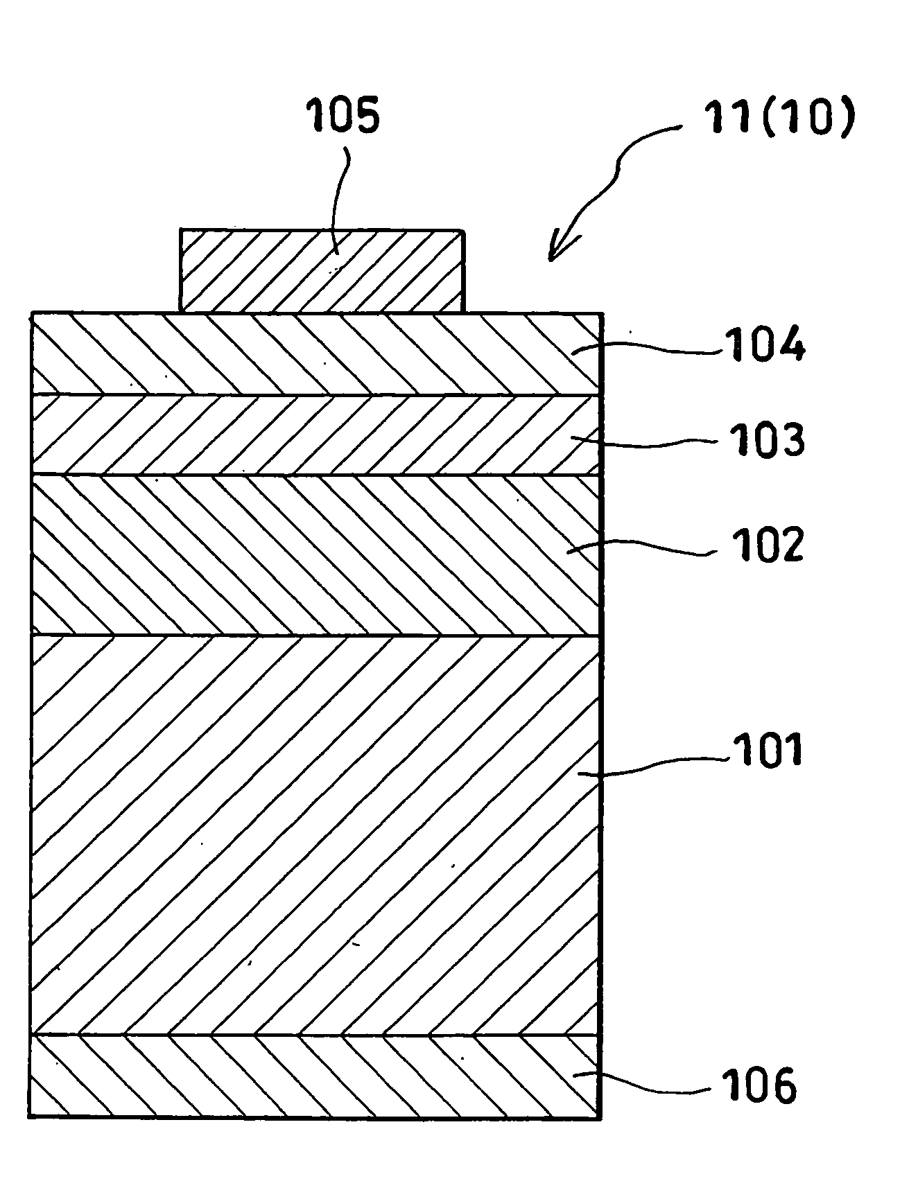
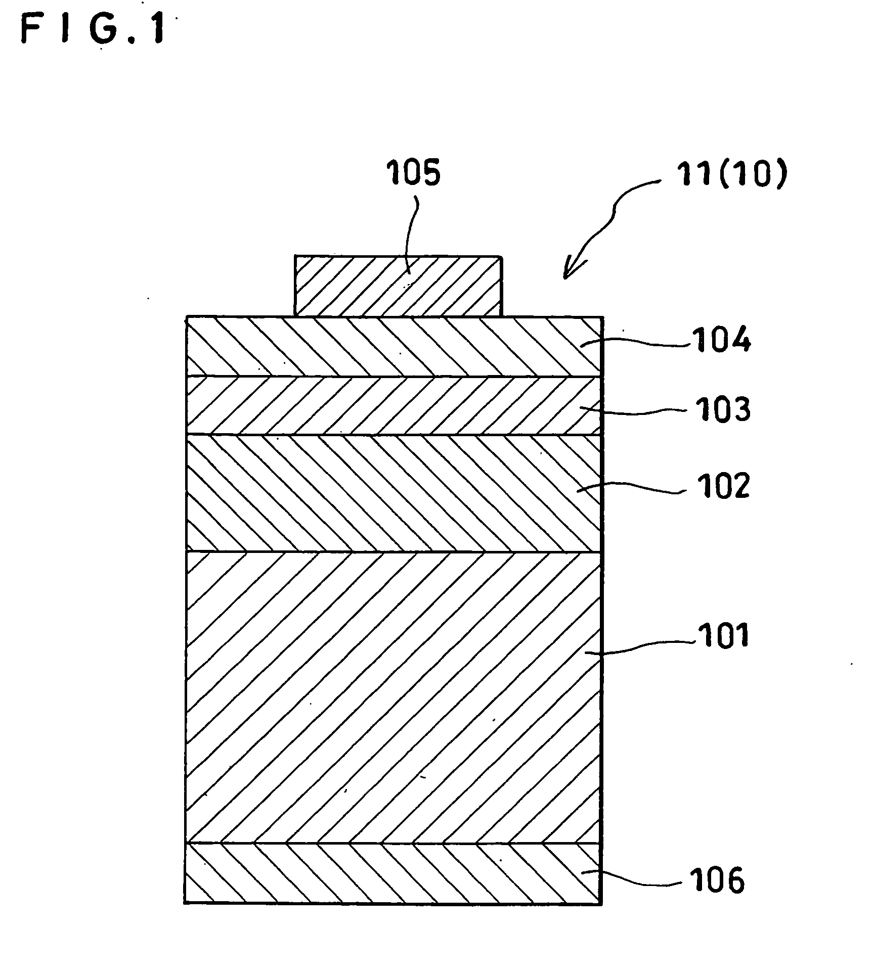
[0044] The present invention will next be described in detail, with reference to fabrication of a boron phosphide-based LED including a (111) boron phosphide (BP) layer formed on a (111) silicon single-crystal substrate and a (0001) gallium indium nitride light-emitting layer formed on the (111) BP layer.

[0045]FIG. 1 schematically shows a cross section of a stacked structure employed for fabricating an LED according to the present invention having a double-hetero (DH) junction structure. In FIG. 1, a stacked structure 11 is provided for fabricating an LED chip 10.

[0046] The stacked structure 11 was formed by sequentially stacking on a phosphorus-doped n-type (111) silicon (Si) single-crystal substrate 101 an undoped n-type (111) boron phosphide lower cladding layer 102, a multi-quantum well structure light-emitting layer 103 including repeatedly (3 times) stacked an n-type (0001) gallium indium nitride (Ga0.90In0.10N) well layer and a (0001) gallium nitride barrier layer, and an u...


PUM


Abstract

A boron phosphide-based semiconductor light-emitting device includes a substrate of silicon single crystal, a first cubic boron phosphide-based semiconductor layer that is provided on a surface of the substrate and contains twins, a light-emitting layer that is composed of a hexagonal Group III nitride semiconductor and provided on the first cubic boron phosphide-based semiconductor layer and a second cubic boron phosphide-based semiconductor layer that is provided on the light-emitting layer, contains twins and has a conduction type different from that of the first cubic boron phosphide-based semiconductor layer.

Description

CROSS REFERENCE TO RELATED APPLICATIONS [0001] This application is an application filed under 35 U.S.C. §111(a) claiming the benefit pursuant to 35 U.S.C. §119(e)(1) of the filing date of Provisional Application No. 60 / 553,531 filed Mar. 17, 2004 pursuant to 35 U.S.C. §111(b).TECHNICAL FIELD [0002] The present invention relates to a boron phosphide-based semiconductor light-emitting device having a boron phosphide-based semiconductor layer exhibiting a wide bandgap, which device can emit high-intensity light in spite of a lattice-mismatch structure thereof. BACKGROUND ART [0003] Conventionally, an n-type or a p-type boron phosphide (BP)-based semiconductor layer has been employed for fabricating light-emitting diodes (LEDs) and laser diodes (LDs). For example, JP-A HEI 5-283744 discloses that a blue-LED is fabricated from a semiconductor structure including a silicon substrate, and an n-type BP layer to which silicon (Si) has been intentionally added and an aluminum gallium nitride ...

Claims


Application Information

Patent Timeline
IPC IPC(8): H01L33/00H01L21/205H01L33/16H01L33/32
CPCH01L33/32H01L33/16
Inventor UDAGAWA, TAKASHI
Owner SHOWA DENKO KK
Why Eureka
Try Eureka