Micro-pattern forming apparatus, micro-pattern structure, and method of manufacturing the same

a technology of micro-patterns and forming apparatus, which is applied in the field of micro-pattern forming apparatus, micro-pattern structure, and manufacturing the same, can solve the problems of inability to peel off the mask, material strength is generally too weak against heat and vacuum to use such a technique as a means of vacuum depositing, and the technique of fine patterning using materials other than inorganic materials is not as well developed, etc., to achieve the effect of enhancing the strength of the mask

Inactive Publication Date: 2007-08-30
RIKEN +1
View PDF5 Cites 30 Cited by
  • Summary
  • Abstract
  • Description
  • Claims
  • Application Information

AI Technical Summary

Benefits of technology

[0020]peeling said mask pattern off from said fluorocarbon layer on said substrate. Thus, with combination of lithography and reactive ion etching, a fine mask with concavity and convexity can be produced.
[0021]In yet another embodiment of the micro-pattern forming apparatus according to the present invention, the fine masking means has a reinforcing rib being made from a photoresis

Problems solved by technology

Whereas techniques for fine patterning using materials other than inorganic materials, such as synthetic organic molecules/macromolecules, organic materials, and biomolecules/biomacromolecules (e.g., protein and DNA) are not as well developed.
These materials are generally too weak against heat and vacuum to use such a technique as a means of vacuum depositing.
Even worse, when the surface of the materials described above is coated with a masking material made from photoresist, for example, in many cases it is impossible to peel off the mask.
These techniques and methods are totally inferior to the patterning techniques for inorganic materials described above, in terms of precision of forming thin layers (films) and patterns.
Silicon nitride thin layers have, howeve

Method used


Image

  • Micro-pattern forming apparatus, micro-pattern structure, and method of manufacturing the same
  • Micro-pattern forming apparatus, micro-pattern structure, and method of manufacturing the same
  • Micro-pattern forming apparatus, micro-pattern structure, and method of manufacturing the same

Examples


embodiment 2

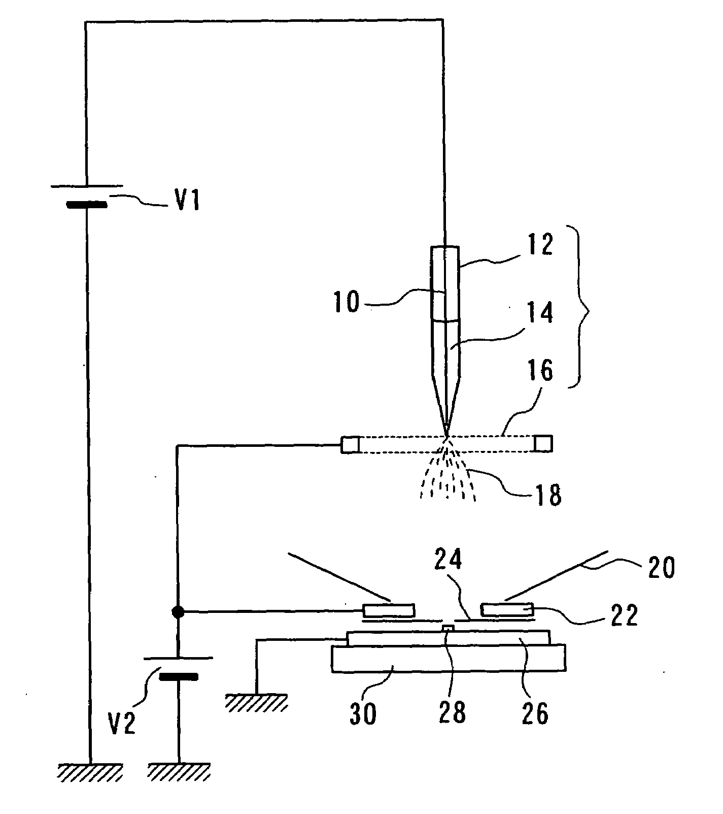
[0076]FIG. 6 is a schematic view showing an example of a basic configuration of a micro-pattern forming device using a vibrator. In FIG. 6 an atomizer (atomizing part) 110, a high-voltage power supply 120, a collimator electrode(s) 130, a fluorocarbon-resin shield 140, a mask(s) 150, a sample holder 160, a chamber (casing) 170, precise control solution supply part 180 and a high-frequency power source 190 are provided. As shown in the figure, the atomizer 110 is mainly composed of a vibrator (i.e., substrate) having a flat surface. Solution of protein is provided on the flat surface of the substrate of the atomizer 110 by precise control solution supply part 180. This solution is charged on the substrate by the predetermined voltage provided by the high-voltage power supply 120. Alternatively, particulate after atomization may be charged. The prescribed high-frequency signal from the high-frequency power source 190 is provided on the substrate of the atomizer 110, so that the signal...

embodiment 3

[0091]FIG. 10 is a photograph in substitution for a drawing showing a SEM micrograph of an organic micro-pattern structure formed by the micro-pattern forming apparatus according to the present invention. Invertase (protein) 2.5 g / L is sprayed in 3 minutes with the micro-pattern forming apparatus by ESD method to form a micro-pattern structure and this SEM micrograph is taken of the formed micro-pattern structure by a high-resolution scanning electron microscope. As shown, it is observed that particles having about 200 nm diameter are obtained.

[0092]FIG. 11 is a SEM micrograph of an organic micro-pattern structure formed by the micro-pattern forming apparatus according to the present invention. Invertase (protein) 0.5 g / L is sprayed / atomized in 30 minutes with the micro-pattern forming apparatus by ESD method to form a micro-pattern structure and this SEM micrograph is taken of the formed micro-pattern structure by a high-resolution scanning electron microscope. As shown, it is obse...


PUM


Abstract

There is provided a micro-pattern forming apparatus including an electrospraying part for applying a voltage to a solution containing a sample to electrostatically atomizing the solution; a supporting part (30) for supporting a chip (26), on which the sample in the solution electrostatically atomized by the electrospraying part, is to be deposited; and a fine mask part (24) disposed between the electrospraying part and the supporting part, having a mask pattern for being passed through by the electrostatically atomized solution in order to form a micro-pattern of the sample upon the chip, wherein the mask pattern is made from a photoresist material with concavity and convexity on the side of the supporting part.

Description

FIELD OF THE INVENTION[0001]The present invention relates to a micro-pattern forming apparatus, a micro-pattern structure, and a method of manufacturing the same. The present invention particularly relates to a micro-pattern forming apparatus to form a micro-pattern of organic materials using a masking means, which is prepared by lithography and reactive ion etching, and the electrospray deposition method, a micro-pattern structure, and a method of manufacturing the same.DESCRIPTION OF THE RELATED ART[0002]Techniques for forming fine patterns on a substrate are widely needed. Especially in the field of semiconductor manufacturing, techniques for patterning thin layers or films of inorganic materials mainly including metal, oxide, and nitride by photoresist masking are quite well developed, and techniques for forming patterns of no more than 100 nm in line width are also known to be already in practice. The means mainly used for these patternings are forming thin layers by vacuum dep...

Claims


Application Information

Patent Timeline
IPC IPC(8): B05D1/32C25D5/00B05C5/00B81C99/00
CPCB01J2219/0036G03F7/12B01J2219/00378B01J2219/00527B01J2219/00585B01J2219/00596B01J2219/00659B01J2219/00725B01L3/0268B01L2300/0819B01L2300/0838B01L2400/027B05B5/025B05B5/087G03F1/20B01J2219/00371
Inventor YAMAGATA, YUTAKAOHMORI, HITOSHIKASE, HIROSHINONAKA, HIROMIKANEKO, AINITTA, KAZUYA
Owner RIKEN
Why Eureka
Try Eureka