Wiring member, resin-coated metal part and resin-sealed semiconductor device, and manufacturing method for the resin-coated metal part and the resin-sealed semiconductor device

Active Publication Date: 2007-09-13
PANASONIC HLDG CORP
View PDF12 Cites 22 Cited by
  • Summary
  • Abstract
  • Description
  • Claims
  • Application Information

AI Technical Summary

Benefits of technology

[0025] A second aim of the present invention is to, by improving adhesion between silicone resin and wiring leads, provide an LED device that can achieve favorable light emitting properties and a manufacturing method for such LED device.
[0063] Note that in the present invention, the organic coating composed of a single-molecule film is formed by the self-assembly of functional organic molecules and has a highly superior bonding property for the wiring leads. While having a single-molecule thickness, the present invention satisfies the demand for enhancing corrosion resistance, rust resistance, and anti-insulating properties of the area of the wiring leads where the organic coating is formed, and furthermore is very space efficient in the device. There is also no need to remove the organic coating after its provision. With respect to such points regarding functionality and structure, the present invention is entirely different from general surface preparation agents, surface activating agents, coating materials, and the like.

Problems solved by technology

However, resin casts in semiconductor devices and LED devices, as well as film carrier tape have the following issues.
The first issue is a problem in which during the injection of the sealing resin, the resin not only fills the intended resin cast area, but also adheres to wiring lead areas that are not part of the intended resin cast area.
Although the dies 91 and 92 may be shaped with higher precision in order to prevent this problem, not only do costs rises significantly due to die designing, but also it is very difficult to completely prevent the occurrence of gaps due to problems with machine precision.
However, the technology disclosed in patent documents 1 and 2 increases the pressure applied to the wiring lead of the dies, and therefore there is the danger of applying an excessive deforming stress to the wiring lead, and there is the fear of damaging the dies or the wiring lead.
However, even if such tape is used, there is the possibility of problems such as detachment of and damage to the tape in the injection step which involves mechanical frictional force under relatively high temperatures.
Moreover, providing the tape still has problems with respect to a decrease in manufacturing efficiency and a rise in manufacturing costs.
This also has problems with respect to a decrease in manufacturing efficiency and a rise in manufacturing costs.
The second issue is a problem when using silicone resin as the sealing resin in an LED device.
Accordingly, there is detachment between the silicone resin and the wiring lead, and there is the possibility of problems such as performance degredation due to poor contact, or insufficient contact strength.
Although there is also a technique of providing an Ag plating on surfaces of the wiring lead in order to improve luminous efficiency in an LED device, there is an issue regarding the Ag plating coat, which is mentioned here as the third issue.
Accordingly, a sufficient reflection coefficient cannot be obtained when a blue, violet, ultraviolet, LED etc. is implemented in an LED device, in which case there is the possibility of not, obtaining an intended luminous efficiency.
There is therefore the possibility of problems with respect to a reduction in the mechanical strength of the film carrier tape after the Sn plating has been performed, and with respect to the plating not being formed evenly.

Method used


Image

  • Wiring member, resin-coated metal part and resin-sealed semiconductor device, and manufacturing method for the resin-coated metal part and the resin-sealed semiconductor device
  • Wiring member, resin-coated metal part and resin-sealed semiconductor device, and manufacturing method for the resin-coated metal part and the resin-sealed semiconductor device
  • Wiring member, resin-coated metal part and resin-sealed semiconductor device, and manufacturing method for the resin-coated metal part and the resin-sealed semiconductor device

Examples


embodiment 1

[0091] 1. Semiconductor Device Structure

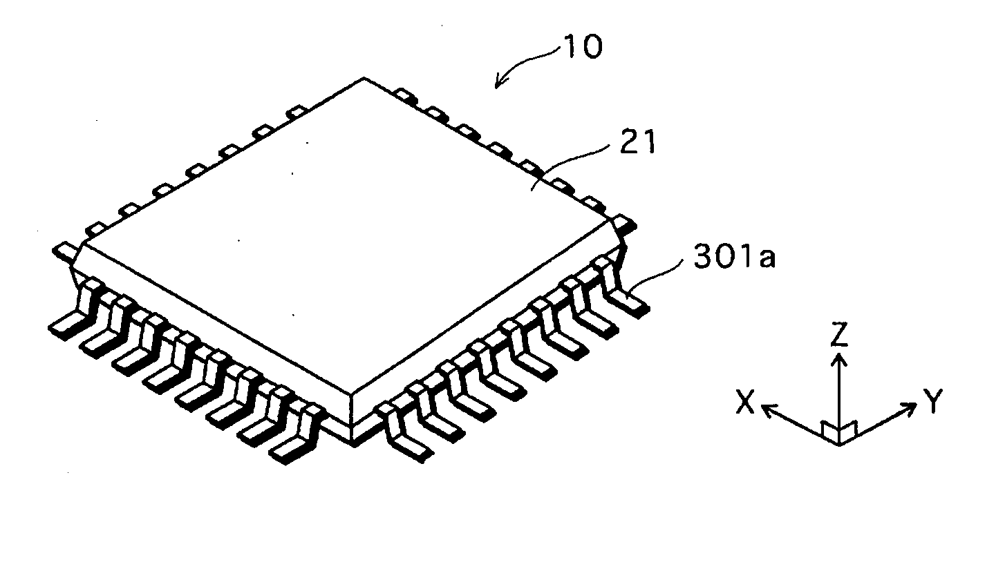
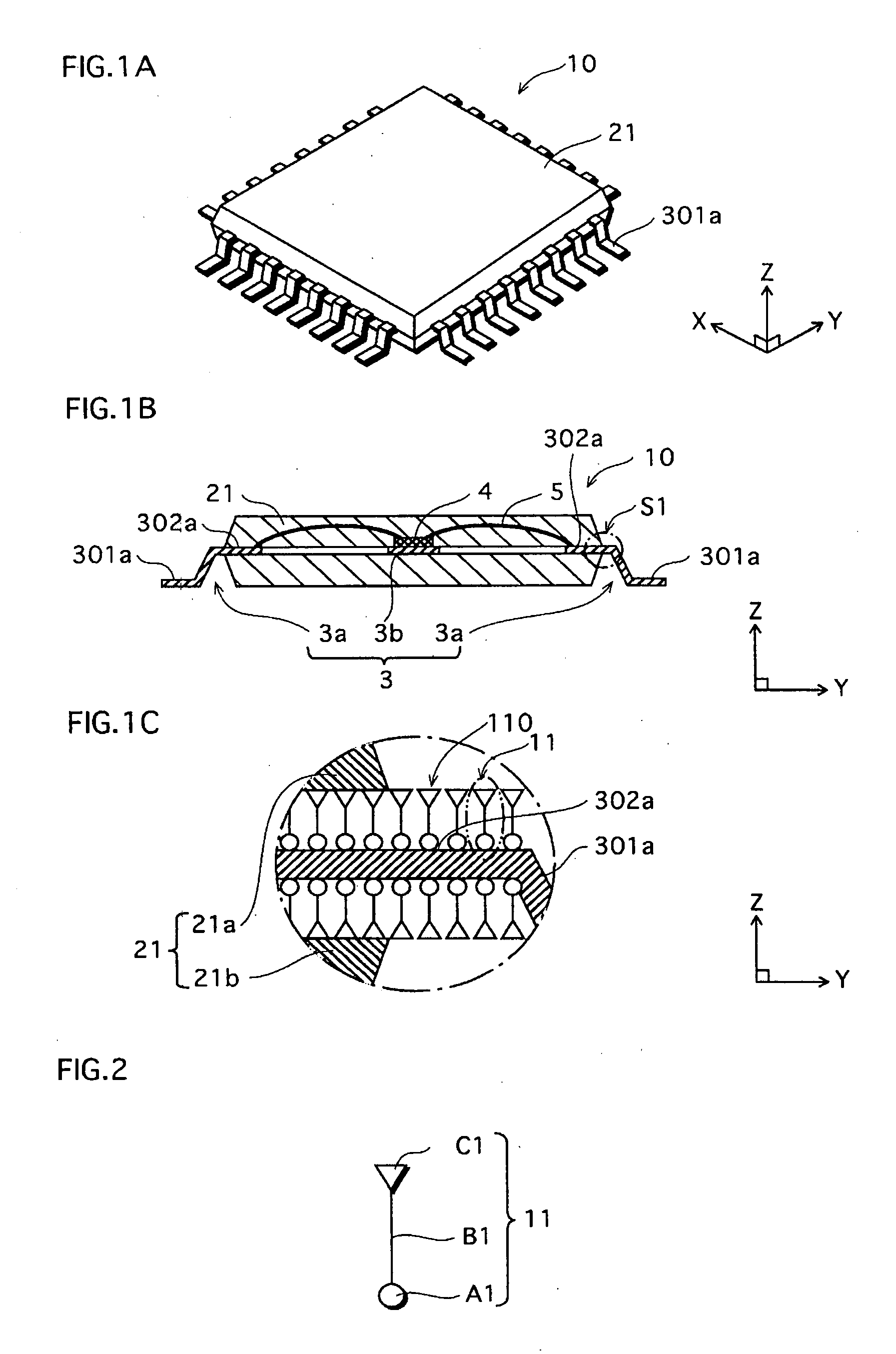
[0092]FIG. 1A is an external perspective view showing a structure of a semiconductor device (QFP 10, Quad Flat Package), which is an exemplary application of the present invention. FIG. 1B is a y-z cross-sectional view of the QFP 10. FIG. 1C is an enlarged view of portion S1 in FIG. 1B.

[0093] The QFP 10 is a surface-mounted semiconductor device used in an IC, LSI etc., and is composed of a semiconductor chip 4, a wiring lead 3, wires 5, a molded resin 21, and the like.

[0094] The wiring lead 3 is constituted from a metallic material that has superior electrical conductivity (e.g., copper alloy), and has a structure that also includes die pads 3a and 3b that have been punched out of a metal plate.

[0095] As shown in FIG. 1A, the QFP 10 has a structure that includes the molded resin 21 formed in a board shape and having a predetermined thickness and square main surface, and outer leads 301a that are a part of the die pads 3a and extend out fro...

embodiment 2

[0157] The organic coating 110 composed of the functional organic molecules 11 pertaining to the present invention has various effects when applied to a semiconductor device as mentioned above, but this is nothing more than one example.

[0158] The existence of a semiconductor chip is not required. For example, the organic coating 110 can be applied to an LED device that includes a light emitting diode (LED) element instead of a semiconductor chip.

[0159]FIG. 7 is a schematic cross-sectional view showing a structure of a wiring lead 30 and a reflector 22 of an LED device unit 31x of embodiment 2 of the present invention.

[0160] In a cross-sectional structure of the LED device unit 31x, the wiring lead 30 has been provided on a bottom portion of the mortar-shaped reflector 22. The reflector 22 is formed by a resin mold using a thermoset resin material (e.g., epoxy resin).

[0161] Similarly to embodiment 1, there is the possibility of resin burrs forming in the LED device unit 31x as we...

embodiment 3

[0167] The following is a description of embodiment 3 of the present invention focusing on differences from embodiment 2.

[0168] LED Device Structure

[0169]FIGS. 8A to 8C are cross-sectional views showing a structure of and manufacturing steps for an LED device 31 pertaining to embodiment 3 of the present invention.

[0170] The LED device 31 basically includes the device unit 31x of embodiment 2, and as shown in FIG. 8B, further includes an LED chip 42 that has been bonded, via a paste 42a, on the wiring lead 30 surrounded by the reflector 22. The LED chip 42 is connected to the wiring lead 30 via the wire 52.

[0171] A transparent sealing resin 82 is filled into the reflector 22 on a reflector surface 201 and the exposed areas 301 and 3102 so as to seal the LED chip 42 and the like.

[0172] Silicone resin, which is one example of a thermoset resin, is used as the sealing resin 82.

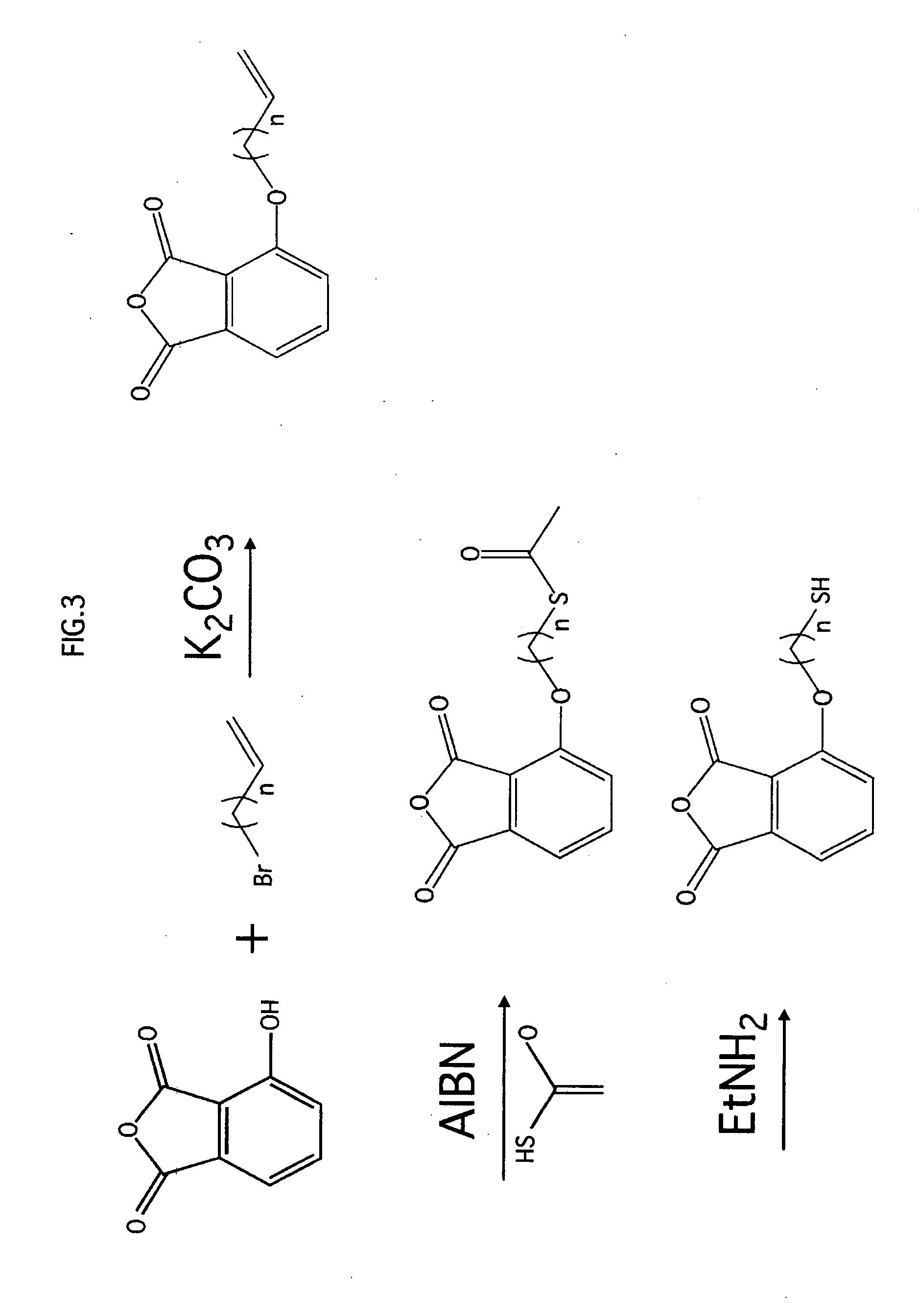
[0173] In embodiment 3, an organic coating 120, which is composed of a single-molecule film formed by the...


PUM

PropertyMeasurementUnit
Metallic bondaaaaaaaaaa
Hardeningaaaaaaaaaa
Surface areaaaaaaaaaaa

Abstract

There is provided a semiconductor device that suppresses the occurrence of resin burrs and has favorable electrical connectivity and bond strength, and a manufacturing method for such semiconductor device. A resin-coated metal part is manufactured by forming an organic coating by depositing a material including functional organic molecules on a wiring lead composed of a metallic material. Each of the functional organic molecules includes a main chain, a first functional group having a metal bonding property, and a second functional group. The first functional group and the second functional group are provided at different ends of the main chain. Thereafter the functional organic molecules self-assemble by bonding of the first functional groups to metal atoms of the wiring lead. After performing the organic coating formation step, resin is adhered to a predetermined surface area of the wiring lead having the organic coating formed thereon.

Description

BACKGROUND OF INVENTION [0001] 1. Field of the Invention [0002] The present invention relates to a wiring member, a resin-coated-metal part and a resin-sealed semiconductor device, and a manufacturing method for the resin-coated metal part and the resin-sealed semiconductor device, and in particular to technology for improving adhesion between a metallic material and a resin material. [0003] 2. Related Art [0004] Resin materials are widely used in semiconductor devices and wiring members. [0005] In general, a semiconductor device such as an integrated circuit (IC) or large scale integrated circuit (LSI) are manufactured by a process in which a predetermined semiconductor element is connected to wiring leads by wire bonding etc., a portion of the wiring leads are exposed to the exterior, and packaging by resin sealing is performed by adhering resin to the wiring leads in this condition. [0006]FIGS. 21A to 21D are schematic cross-sectional diagrams showing manufacturing steps for a re...

Claims


Application Information

Patent Timeline
IPC IPC(8): H05K3/00H01L33/50H01L33/54H01L33/56H01L33/62
CPCB29C39/10Y10T428/29B29L2011/0083H01L21/565H01L23/3135H01L23/49503H01L23/49586H01L33/52H01L33/54H01L33/56H01L2224/48091H01L2224/48247H01L2924/01003H01L2924/01005H01L2924/01011H01L2924/01015H01L2924/01027H01L2924/01029H01L2924/01046H01L2924/01047H01L2924/0105H01L2924/01061H01L2924/01078H01L2924/01079H01L2924/01082H01L2924/14H01L2924/1433H05K3/28H05K3/389B29L2011/00H01L24/29H01L2924/01045H01L2924/01044H01L2924/01033H01L2924/01019H01L2924/01006H01L2224/73265H01L24/32H01L24/48H01L2224/32245H01L2924/00014H01L2924/00012H01L2924/3512H01L2924/00H01L24/73H01L2924/12041H01L2924/181Y10T428/31522Y10T428/31678H01L2224/45099H01L2224/45015H01L2924/207
Inventor FUKUNAGA, TAKAHIROIMURA, RYOUTAROU
Owner PANASONIC HLDG CORP
Why Eureka
Try Eureka