

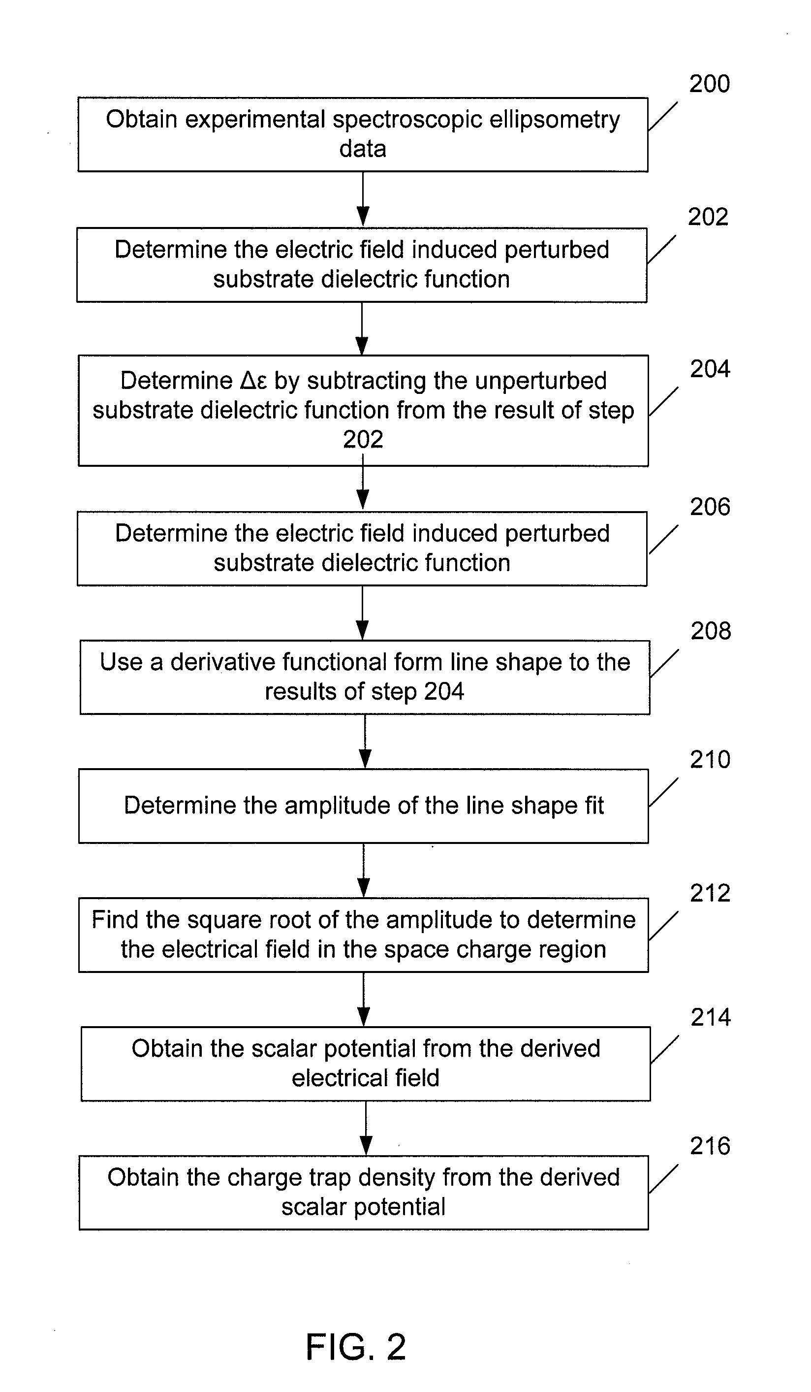
Methods and Systems for Determining Trapped Charge Density in Films
a technology of trapped charge density and film, applied in the field of semiconductor/solid-state device testing/measurement, can solve the problems of poor transistor drive current due to degraded field effect carrier mobility, inability to determine the extent of charge trapping, and inability to achieve the effect of determining the accuracy o
- Summary
- Abstract
- Description
- Claims
- Application Information
AI Technical Summary
Benefits of technology
Problems solved by technology
Method used
Image

Examples
example 1
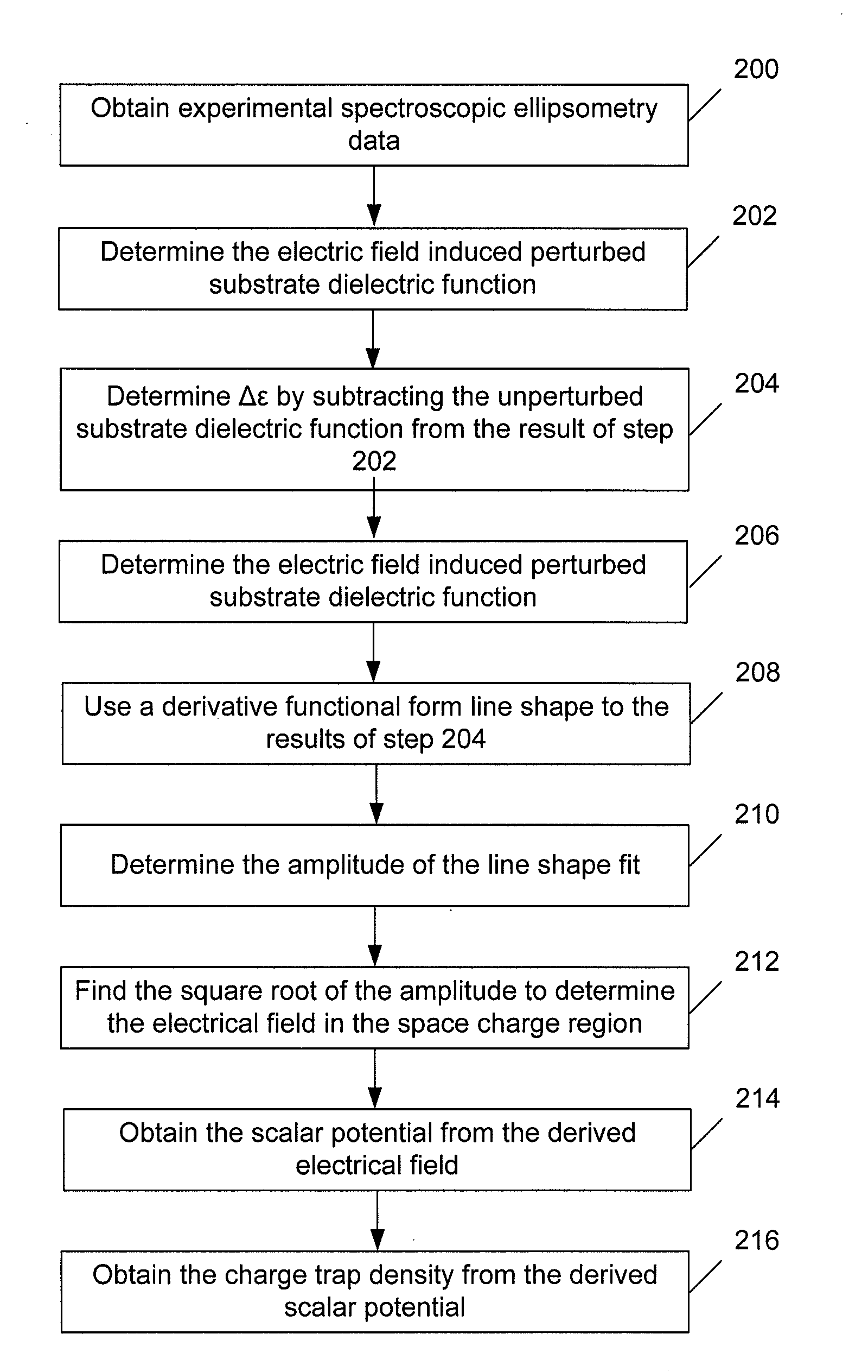
[0062]A first sample with substantially less charge trap density at the interface (e.g., HF cleaned silicon surface without a HfO2 film with a typical charge trap density of about 1×1010 cm−2 to 5×1010 cm−2) and a second sample with an expected high density of charge traps at the interface are tested using techniques of the present disclosure (e.g., using the steps described in FIG. 2). In particular, the first sample includes a (100)-oriented silicon surface (HF cleaned surface) having about 1.4 nanometers silicon dioxide (SiO2) layer. The second sample with the expected high density of charge traps includes a (100) silicon surface (HF cleaned surface) with an atomic layer deposited HfO2 layer having a thickness of about 3 nm and a typical charge trap density values of about 1×1011 cm−2 to 5×1011 cm−2.
[0063]Referring to FIG. 8, the amplitude of the silicon sample with the HfO2 layer (800) is about twice much as the silicon sample with silicon dioxide (802), as expected due to the a...
example 2
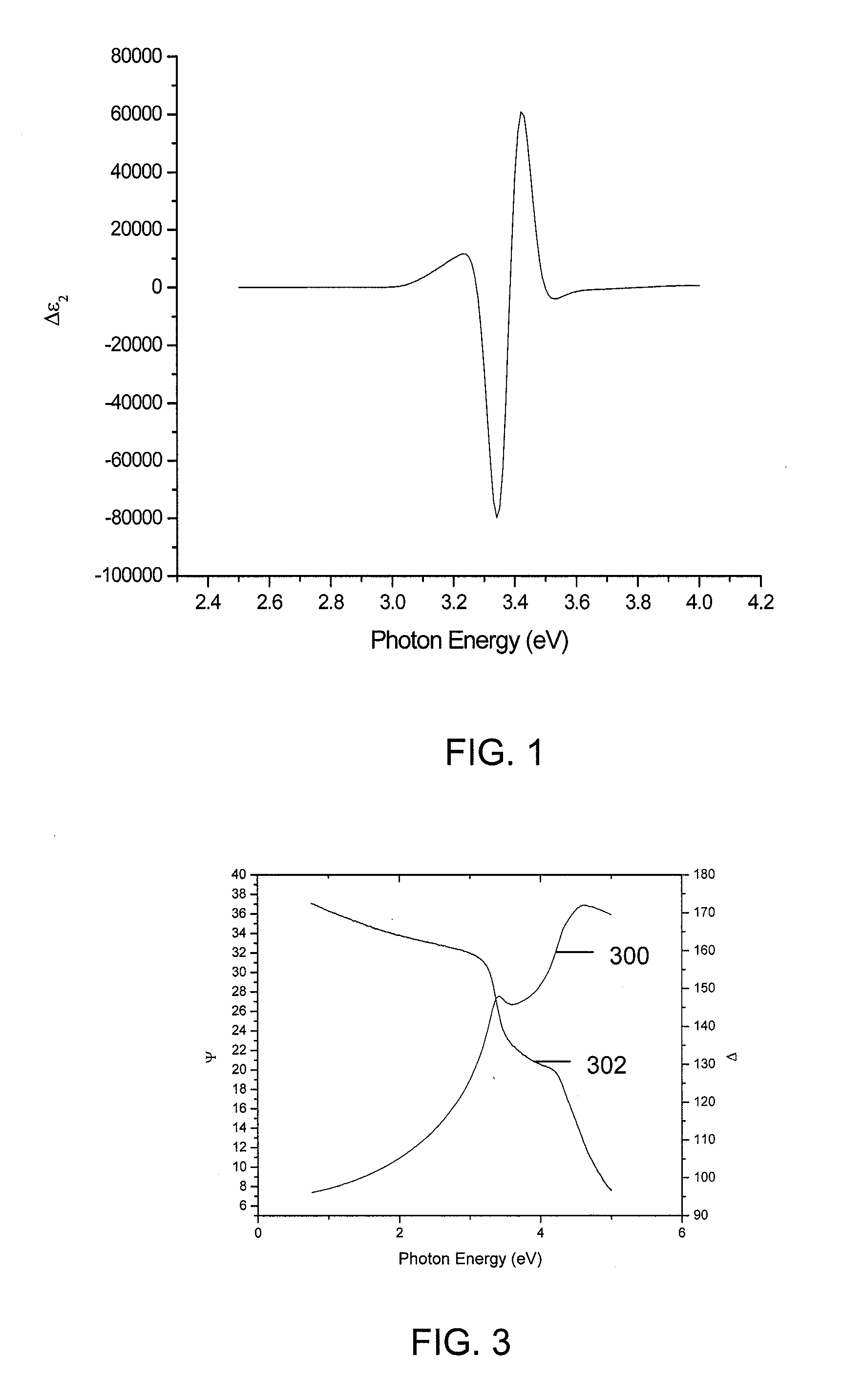
[0065]This example provides a correlation to second harmonic generation (SHG) results. First, five (100) silicon substrates were prepared with an initial HF last treatment followed by growth of the SiO2 interlayer using ozonated (O3) water (HCl 0.2%) using techniques known in the art. Following the surface clean, a 45% silicate (HfSiO) gate dielectric was deposited via atomic layer deposition (ALD) on each wafer. One wafer (wafer 900 of FIG. 9) was left as-deposited and received no further post deposition anneals, while the remaining four wafers were annealed in an NH3 ambient at 600° C. (wafer 902), 700° C. (wafer 904), 800° C. (wafer 906), and 900° C. (wafer 908). Spectroscopic ellipsometry data was taken on a J.A. Woollam Co. ellipsometer over the spectroscopic range of 0.75 eV −5.0 eV by 0.02 eV increments and an angle of incidence of 70-78 degrees by 4 degree increments.
[0066]The method of the present disclosure, for example, the method outlined in FIG. 2 was performed on each ...
example 3
[0068]The following example shows a correlation between electrical results indicating sensitivity and identifying charge traps. The samples include three gate dielectrics (HfO2, HfTiO, and HfTaTiO) formed by oxidizing the physical vapor deposition (PVD) metals (Hf, Ti, and Ta, respectively) with post-deposition anneals (PDAs). Each of the three gate dielectric was formed on a separate 8-inch, (100) silicon surface treated with hydrofluoric acid (“HF-Last”). After the metal deposition, a portion of each wafer was subsequently annealed (PDA) at 900° C. for 30 seconds in a N2 ambient for the SE measurement. These samples were measured using a J. A. Woollam spectroscopic ellipsometer. In particular, the measurements were taken at two angles of incidence, 70° and 76°, across a 0.75-6.55 eV spectroscopic range with a scanning step size of 0.05 eV.
[0069]The electrical measurements were performed in which the gate is tied to a pulse generator, the substrate grounded, and the source and drai...
PUM
 Abstract
Description
Claims
Application Information