Semiconductor quantum dot device

a quantum dot and semiconductor technology, applied in semiconductor devices, lasers, semiconductor lasers, etc., can solve the problems of reducing light emission efficiency, quantum dot lasers with operating speed exceeding that of semiconductor lasers, and structure or quantum well structure has not yet been proposed, so as to suppress the increase in the relaxation time of carriers

Inactive Publication Date: 2007-09-20
NEC CORP
View PDF9 Cites 9 Cited by
  • Summary
  • Abstract
  • Description
  • Claims
  • Application Information

AI Technical Summary

Benefits of technology

[0023] The quantum dot device of the present invention is a construction in which a p-type impurity is injected into quantum dots, whereby this p-type impurity causes the generation of holes inside the quantum dots, these holes being at the ground level of the valence band of the quantum dots. In such a construction, the relaxation of carriers (carrier injection) from an excited level to the ground level is accelerated, and increase in the relaxation time of the carriers is therefore suppressed. As a result, the modulation band of the quantum dot device can be extended and a broad modulation band on the order of 10 GHz or more and an operating speed on the order of 10 GHz or higher can be realized.

Problems solved by technology

However, these methods have the drawback that processing damage which occurs in the semiconductor crystal as a result of lithography or dry etching greatly reduces the light emission efficiency.
However, a quantum dot laser which has an operating speed surpassing that of a semiconductor laser of the prior art having an active layer of bulk structure or quantum well structure has not yet been proposed.
This is due to problems described hereinbelow that are inherent to quantum dots.
As a result, if the ground levels of the conduction band and valence band are already occupied by conduction electrons and holes (carriers), additional conduction electrons or holes cannot be injected in the ground level.
As is obvious from the foregoing explanation, the modulation rate in a quantum dot device such as a quantum dot laser drops due to decrease in the relaxation rate of carriers (increase in carrier relaxation time τ2-1), and this limited modulation rate complicates the realization of a modulation bandwidth on the order of 10 GHz, which is required in a current optical communication system.

Method used


Image

  • Semiconductor quantum dot device
  • Semiconductor quantum dot device
  • Semiconductor quantum dot device

Examples


first embodiment

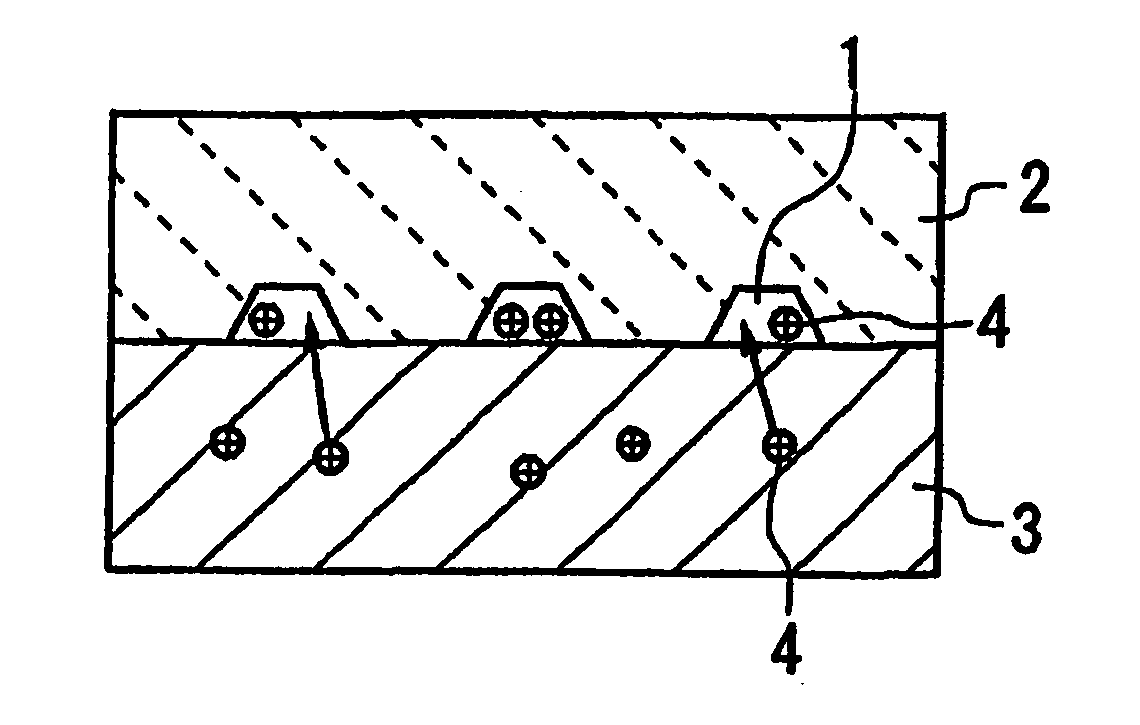
[0049] As shown in FIG. 4A, the semiconductor quantum dot device according to the first embodiment is a construction in which a plurality of quantum dots 1 which have been formed from an undoped semiconductor are disposed on the surface of p-type semiconductor barrier layer 3 at a surface density of, for example, 5×10 cm−2.

[0050] P-type impurity is injected into p-type semiconductor barrier layer 3, whereby a multiplicity of holes 4 exist in the interior of p-type semiconductor barrier layer 3. A portion of these holes 4 are introduced into adjacent quantum dots 1. In other words, this is a construction in which quantum dots 1 shown in FIG. 4A contain holes 4 even though these quantum dots 1 are not injected with p-type impurity (i.e., the quantum dots are undoped). As shown in FIG. 4B, these holes 4 are in the ground level of the valence band of quantum dots 1, and the ground level of the valence band is therefore filled by holes 4. In addition, quantum dots 1 are covered by undop...

second embodiment

[0076]FIG. 7A is a view showing the construction of the second embodiment of the semiconductor quantum dot device according to the present invention, and FIG. 7B is an energy band diagram of this quantum dot device.

[0077] The quantum dot device of the second embodiment is a construction in which quantum dots 1 are formed on undoped semiconductor barrier layer 3a, and p-type semiconductor barrier layer (p-type impurity region) 2a is formed on quantum dots 1. Holes 4 which are generated by the p-type impurity introduced into p-type semiconductor barrier layer 2a are introduced into quantum dots 1. In the quantum dot device according to this second embodiment as well, action and effects can be obtained that are equivalent to the action and effects of the first embodiment.

[0078] In addition, although examples were presented in above-described the first and second embodiments in which a p-type impurity is doped in a semiconductor barrier layer (p-type impurity region) which is disposed...

examples

[0079] Explanation next regards examples of the present invention with reference to the accompanying drawing.


PUM


Abstract

A p-type semiconductor barrier layer is provided in the vicinity of undoped quantum dots, and holes in the p-type semiconductor barrier layer are injected in advance in the ground level of the valence band of the quantum dots. Lowering the threshold electron density of conduction electrons in the ground level of the conduction band of quantum dots in this way accelerates the relaxation process of electrons from an excited level to the ground level in the conduction band.

Description

TECHNICAL FIELD [0001] The present invention relates to electronic devices such as field effect transistors and single-electron elements as well as to semiconductor optical devices such as semiconductor lasers, semiconductor amplifiers, semiconductor optical switches, wavelength conversion elements, and optical memories which are used in, for example, optical communication and optical interconnections; and more particularly to a semiconductor quantum dot device which is provided with quantum dots. BACKGROUND ART [0002] Quantum dots can be called boxes of quantized potential on the hyperfine scale in which carriers (conduction electrons and holes) are confined in three dimensions. The density of the state function of carriers in a quantum dot is broken up according to a delta function, and the injected carriers are concentrated in these discrete energy levels. As a result, light which is emitted when the conduction electrons and holes recombine in the interior of quantum dots is of h...

Claims


Application Information

Patent Timeline
Patent Type & Authority Applications(United States)
IPC IPC(8): H01L31/00H01L29/06H01S5/12H01S5/34H01S5/343
CPCB82Y20/00H01S5/3412H01S5/341H01S5/1228
Inventor SAITO, HIDEAKI
Owner NEC CORP
Why Eureka
Try Eureka