Plasma etching method and computer-readable storage medium

a technology of etching method and computer, applied in the direction of electrical equipment, basic electric elements, electric discharge tubes, etc., can solve the problems of deteriorating operation speed, reducing propagation speed, increasing inter-wiring capacitance, etc., to promote plasma diffusion, increase the etching rate, and improve the effect of etching ra

Inactive Publication Date: 2007-09-20
TOKYO ELECTRON LTD
View PDF15 Cites 14 Cited by
  • Summary
  • Abstract
  • Description
  • Claims
  • Application Information

AI Technical Summary

Benefits of technology

[0016]In accordance with the present invention, when the trench is formed on the substrate or on the film thereon such as the interlayer insulating film or the like, a plasma is generated by applying a high frequency power to either of the first and the second electrode. Further, a DC voltage is also applied to either of the electrodes, so that the plasma is also generated by the DC voltage. Accordingly, a plasma density is increased to thereby enhance the etching rate. In this case, even when using a high frequency power, the plasma density in the central portion can be relatively increased to promote a plasma diffusion. Hence, even if an etching gas is an electronegative gas, the etching rate can be increased in the central portion where the plasma density tends to be low in case an etching gas is an electronegative gas, so that a uniform etching can be performed.

Problems solved by technology

In a semiconductor device, a miniaturization reduces a distance between wirings, and this causes an increase in an inter-wiring capacitance.
Therefore, a signal propagation speed is reduced, thereby deteriorating an operating speed.
However, when these trenches are formed, it is not possible to stop the etching by different kinds of films, so that the etching depth is likely to be formed unevenly.
However, since an etching rate in other portions is also changed, the etching rate distribution becomes W-shaped or M-shaped, making it difficult to obtain the etching uniformity required for the trench etching.
Moreover, although a low power etching is desired in the trench etching, the etching rate is difficult to be controlled by adjusting the conventional parameters in the low power etching process.

Method used


Image

  • Plasma etching method and computer-readable storage medium
  • Plasma etching method and computer-readable storage medium
  • Plasma etching method and computer-readable storage medium

Examples


Embodiment Construction

[0030]Hereinafter, an embodiment of the present invention will be described in detail with reference to the accompanying drawings.

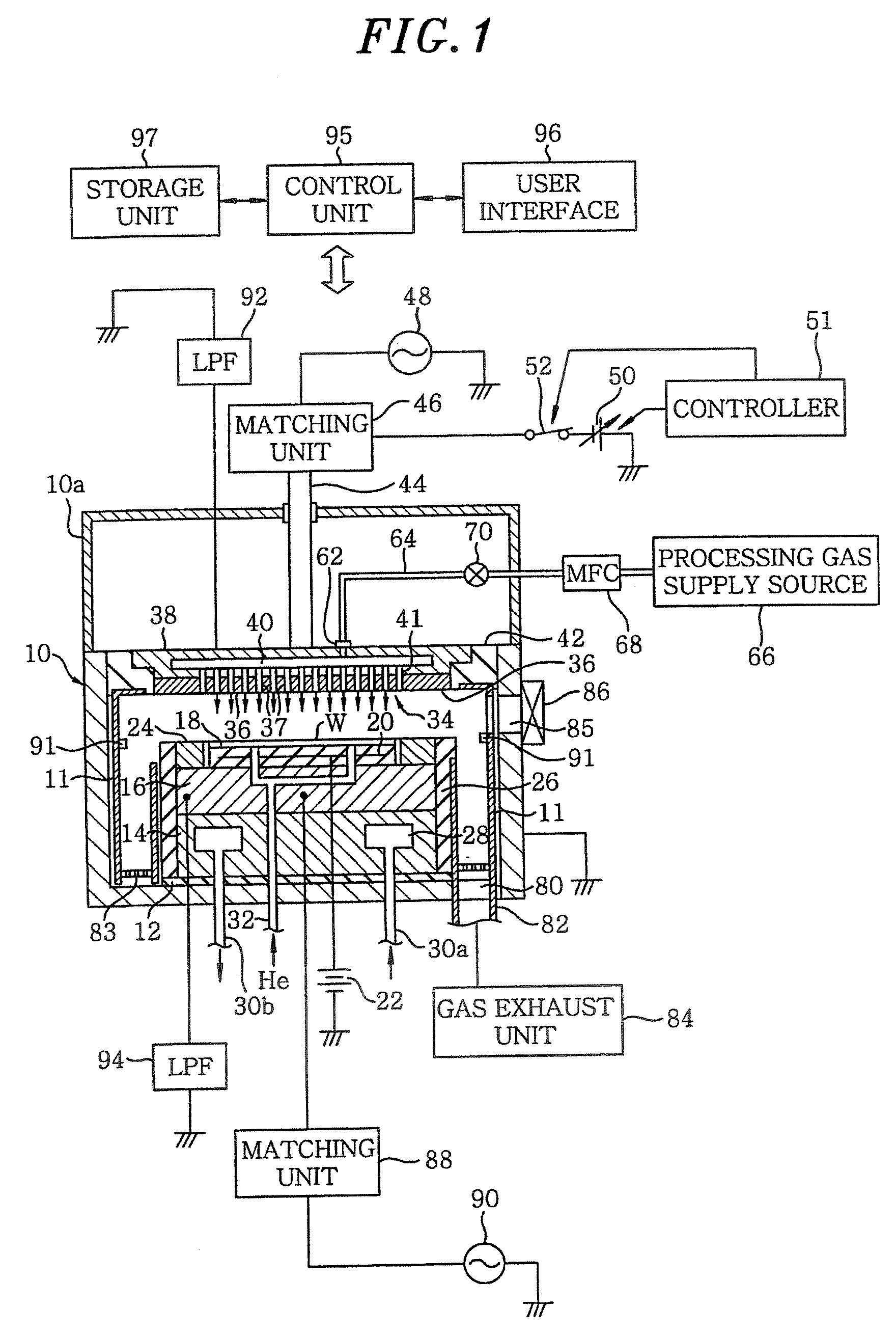
[0031]FIG. 1 is a schematic view showing one example of a plasma etching apparatus utilized in implementing the present invention.

[0032]This plasma etching apparatus is a capacitance-coupled parallel plate type plasma etching apparatus and includes a generally cylindrical chamber (processing chamber) 10 made of, e.g., surface-anodized aluminum. The chamber 10 is a frame-grounded.

[0033]On a bottom portion of the chamber 10, there is arranged a cylindrical susceptor base 14 through an insulating plate 12 made of ceramics or other materials. A susceptor 16 made of, e.g., aluminum, is provided on the susceptor base 14, wherein the susceptor 16 is adapted to serve also as a lower electrode. A semiconductor wafer W serving as an object substrate is mounted on the susceptor (lower electrode) 16.

[0034]On a top surface of the susceptor 16, there is provided an ele...


PUM


Abstract

A plasma etching method for forming a trench on a substrate or on a film formed on the substrate, includes an substrate arranging step of arranging the substrate on which the trench is to be formed in a processing chamber having therein a first and a second electrode disposed to face each other vertically; a processing gas introducing step of introducing a processing gas for etching into the processing chamber; a plasma generating step of generating a plasma by applying a high frequency electric power to either of the first and the second electrode; and a DC voltage applying step of applying a DC voltage to said either of the electrodes. Further, a computer-readable storage medium stores therein a computer-executable control program, wherein, when the control program is being executed, a computer is made to control a plasma processing apparatus to perform the plasma etching method.

Description

FIELD OF THE INVENTION[0001]The present invention relates to a plasma etching method and a computer-readable storage medium for forming a trench on a substrate or on a film formed thereon such as an interlayer insulating film.BACKGROUND OF THE INVENTION[0002]In a semiconductor device, a miniaturization reduces a distance between wirings, and this causes an increase in an inter-wiring capacitance. Therefore, a signal propagation speed is reduced, thereby deteriorating an operating speed. To solve the above problem, an insulating material having a low dielectric constant (low-k material) has been recently used as an interlayer insulating film. Further, copper, which has low resistance and high electromigration tolerance, has been noticed as a wiring material. Furthermore, a dual damascene method is often used to form a connecting opening or a groove wiring of copper.[0003]When a multilayer interconnection of copper is formed by using the dual damascene method, firstly, an etching stop...

Claims


Application Information

Patent Timeline
Patent Type & Authority Applications(United States)
IPC IPC(8): H01L21/465
CPCH01J37/32027H01J37/32082H01L21/7681H01L21/76804H01L21/31116
Inventor YOSHIDA, RYOICHI
Owner TOKYO ELECTRON LTD
Why Eureka
Try Eureka