Graded index silicon geranium on lattice matched silicon geranium semiconductor alloy

a technology of lattice and silicon geranium, which is applied in the direction of chemically reactive gas growth, crystal growth process, polycrystalline material growth, etc., can solve the problems of difficult high-quality (i.e. defect-free) sige layer on silicon substrate, thick growth of thick silicon geranium, etc., and achieves the effect of improving performan

Active Publication Date: 2007-09-27
NASA
View PDF10 Cites 30 Cited by
  • Summary
  • Abstract
  • Description
  • Claims
  • Application Information

AI Technical Summary

Benefits of technology

[0013] Accordingly, it is an object of the present invention to provide a lattice matched silicon germanium (SiGe) semiconductive structure having improved performance when a strained layer is deposited thereon.

Problems solved by technology

However, the growth of thick (i.e., greater than tens of nanometers), high-quality (i.e., defect free) SiGe layers on a silicon substrate is difficult because SiGe has a larger lattice constant than silicon.
This means that the SiGe layers close to the silicon substrate are strained while severe defects (e.g., threading dislocations, micro twins, cracks, delaminations, etc.) develop in the layers of SiGe that exceed the critical thickness of hundreds of nanometers because of the lattice mismatch.
However, the strained layer presents an abrupt transition on the lattice matched SiGe that causes (i) misfit dislocations, (ii) an electric potential barrier at the interface between the lattice matched SiGe and the strained layer, (iii) an abrupt change in refractive index, (iv) an abrupt bandgap change, (v) generation of interfacial mid-bandgap states, and (vi) abrupt strain build-up that tends to attract other atoms to thereby introduce impurities into the device.

Method used


Image

  • Graded index silicon geranium on lattice matched silicon geranium semiconductor alloy
  • Graded index silicon geranium on lattice matched silicon geranium semiconductor alloy
  • Graded index silicon geranium on lattice matched silicon geranium semiconductor alloy

Examples


Embodiment Construction

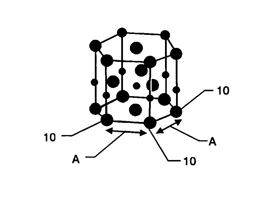
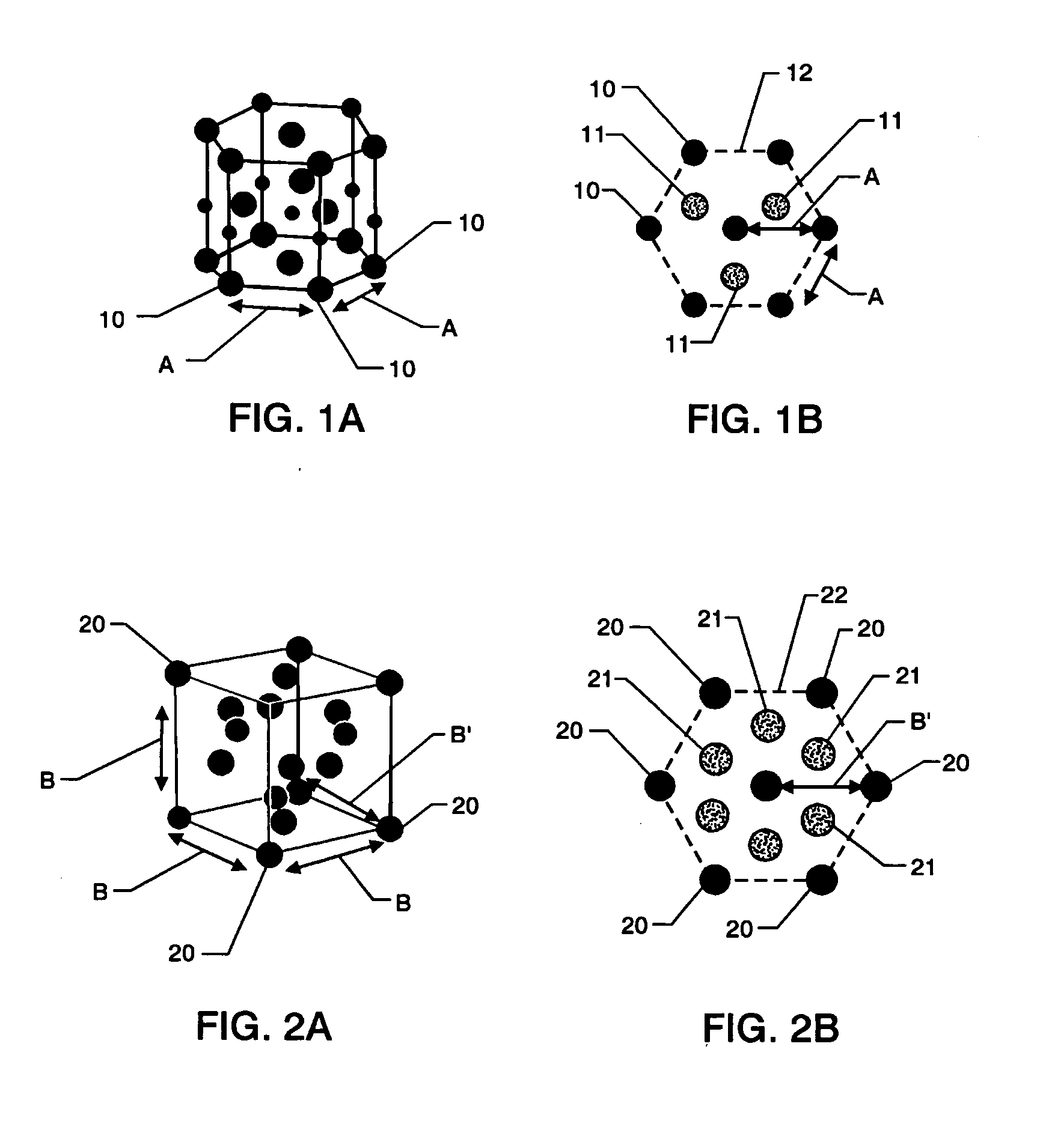
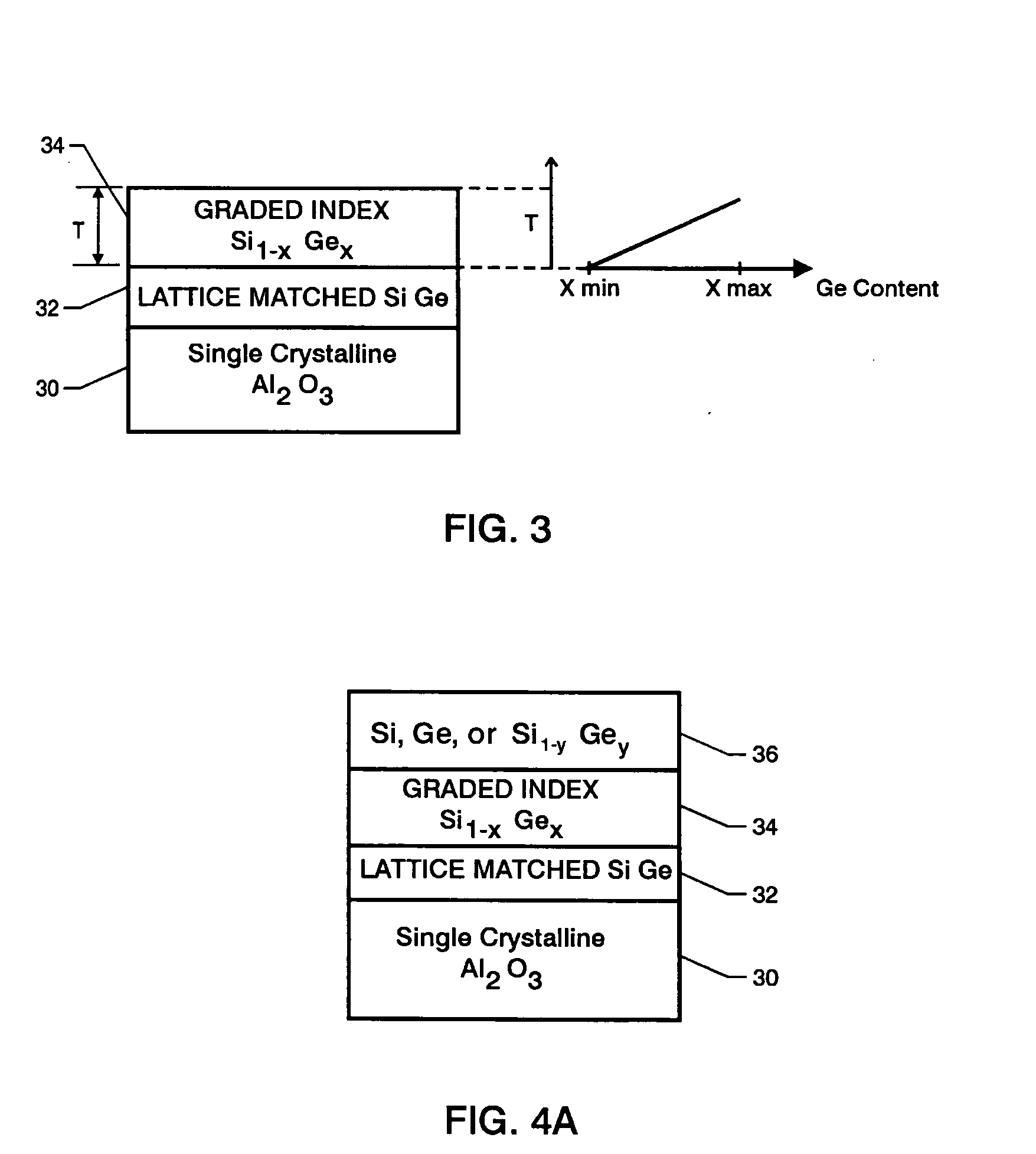
[0025] The silicon germanium (SiGe)-based semiconductive structure of the present invention includes a high-quality (i.e., free of defects and dislocations) silicon germanium (SiGe) semiconductive alloy. The SiGe semiconductive alloy and the fabrication thereof are described in detail in the above-referenced patent application Ser. No. 11 / 242,415, filed Sep. 27, 2005, the entire contents of which are incorporated by reference and will be repeated herein below. The improved SiGe semiconductive alloy fabrication involves growing a cubic diamond structure SiGe on a trigonal crystal structure of single crystalline aluminum oxide (Al2O3) sapphire referred to hereinafter as “single crystalline Al2O3”. The goal of zero defect / dislocations in this SiGe semiconductive alloy is achieved by arranging for a lattice match between the cubic diamond structure SiGe and the single crystalline Al2O3. In order to explain the lattice matching, reference will now be made to FIGS. 1A-1B and FIGS. 2A-2B. ...


PUM

PropertyMeasurementUnit
cut anglesaaaaaaaaaa
lattice constantaaaaaaaaaa

Abstract

A lattice matched silicon germanium (SiGe) semiconductive alloy is formed when a {111} crystal plane of a cubic diamond structure SiGe is grown on the {0001} C-plane of a single crystalline Al2O3 substrate such that a <110> orientation of the cubic diamond structure SiGe is aligned with a <1,0,−1,0> orientation of the {0001} C-plane. A lattice match between the substrate and the SiGe is achieved by using a SiGe composition that is 0.7223 atomic percent silicon and 0.2777 atomic percent germanium. A layer of Si1-xGex is formed on the cubic diamond structure SiGe. The value of X (i) defines an atomic percent of germanium satisfying 0.2277<X<1.0, (ii) is approximately 0.2777 where the layer of Si1-xGex interfaces with the cubic diamond structure SiGe, and (iii) increases linearly with the thickness of the layer of Si1-xGex.

Description

ORIGIN OF THE INVENTION [0001] The invention was made in part by employees of the United States Government and may be manufactured and used by or for the Government of the United States of America for governmental purposes without the payment of any royalties thereon or therefor. BACKGROUND OF THE INVENTION [0002] 1. Field of the Invention [0003] This invention relates to semiconductive structures made from silicon germanium. More specifically, the invention is a lattice matched silicon germanium semiconductive alloy having at least one graded index silicon germanium layer deposited thereon. [0004] 2. Description of the Related Art [0005] Silicon germanium (SiGe) is an important semiconductive alloy used in Field Effect Transistors (FETs), High Electron Mobility Transistors (HEMTs), Hetero Bi-polar Transistors (HBTs), Thermo-Electric (TE) devices, photovoltaic solar cells, and photon detectors. Typically, SiGe is grown on common silicon wafer substrates. However, the growth of thick...

Claims


Application Information

Patent Timeline
Patent Type & Authority Applications(United States)
IPC IPC(8): H01L31/117
CPCC30B25/02C30B29/52H01L21/0242H01L21/02532H01L21/02502H01L21/02507H01L21/0251H01L21/0245
Inventor PARK, YEONJOONCHOI, SANG H.KING, GLEN C.ELLIOTT, JAMES R. JR.STOAKLEY, DIANE M.
Owner NASA
Why Eureka
Try Eureka