High efficiency intersubband semiconductor lasers

a semiconductor laser and high-efficiency technology, applied in semiconductor lasers, laser cooling arrangements, laser details, etc., can solve the problems of low power conversion efficiency (2.5%), severely restricting device design, and very inefficient transitions

Active Publication Date: 2007-10-25
WISCONSIN ALUMNI RES FOUND
View PDF64 Cites 23 Cited by
  • Summary
  • Abstract
  • Description
  • Claims
  • Application Information

AI Technical Summary

Benefits of technology

[0005] In accordance with the present invention, semiconductor lasers are formed to provide highly efficient emission at selected wavelengths, which may lie in the mid- to far-infrared range. Such semiconductor lasers constructed to emit in the infrared range provide efficient conversion of e

Problems solved by technology

Since the radiative transitions are very inefficient the electrons are recycled by using multiple stages.
More recently continuous wave (CW) operation has been achieved at 300 K, but with very low power conversion efficiency (<2.5%) and only at wavelengths between 4.8 and 9 μm.
This fact severely restricts the device design.
Furthermore, for such devices the necessary impurity doping in the superlattice injectors causes a s

Method used


Image

  • High efficiency intersubband semiconductor lasers
  • High efficiency intersubband semiconductor lasers
  • High efficiency intersubband semiconductor lasers

Examples


Embodiment Construction

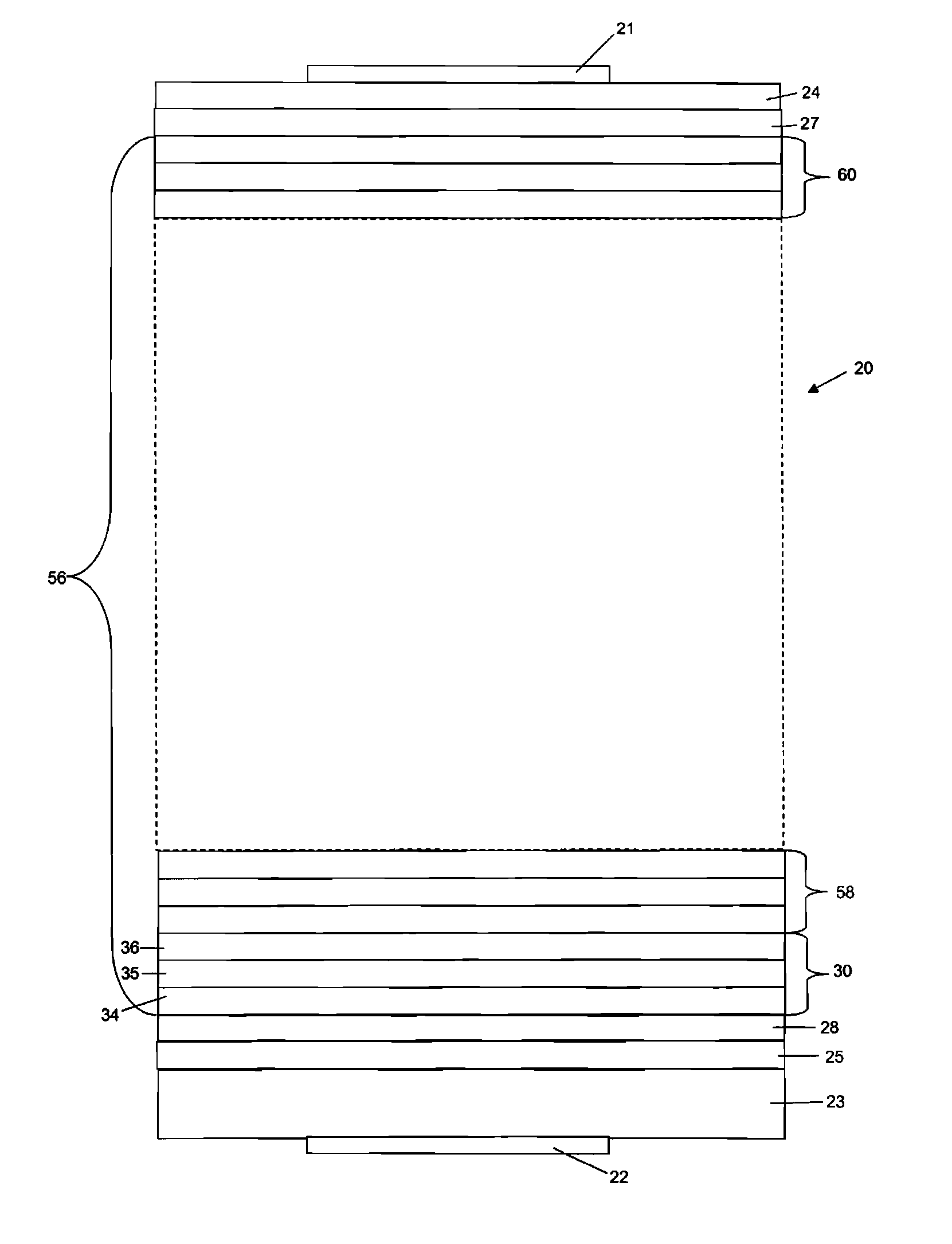
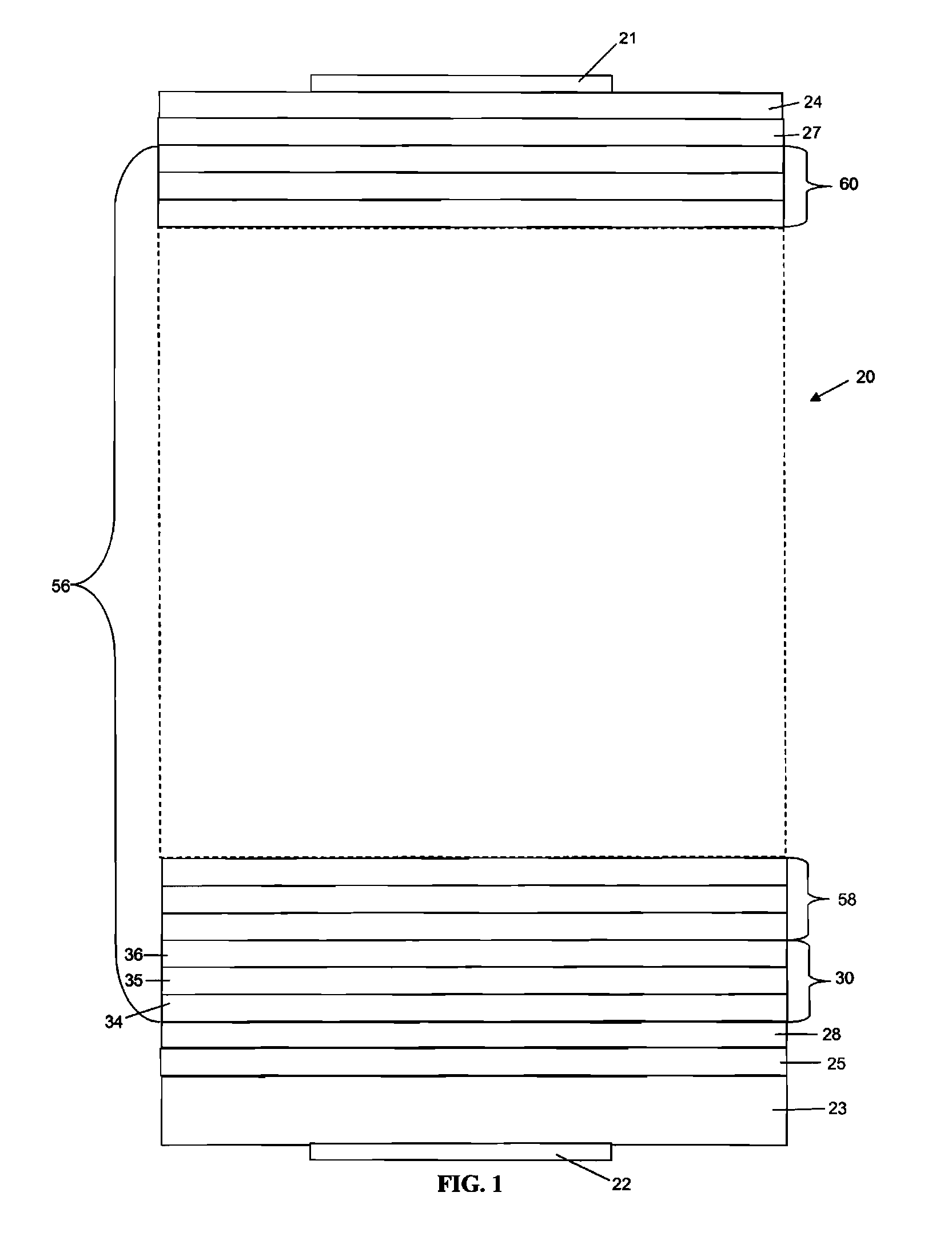
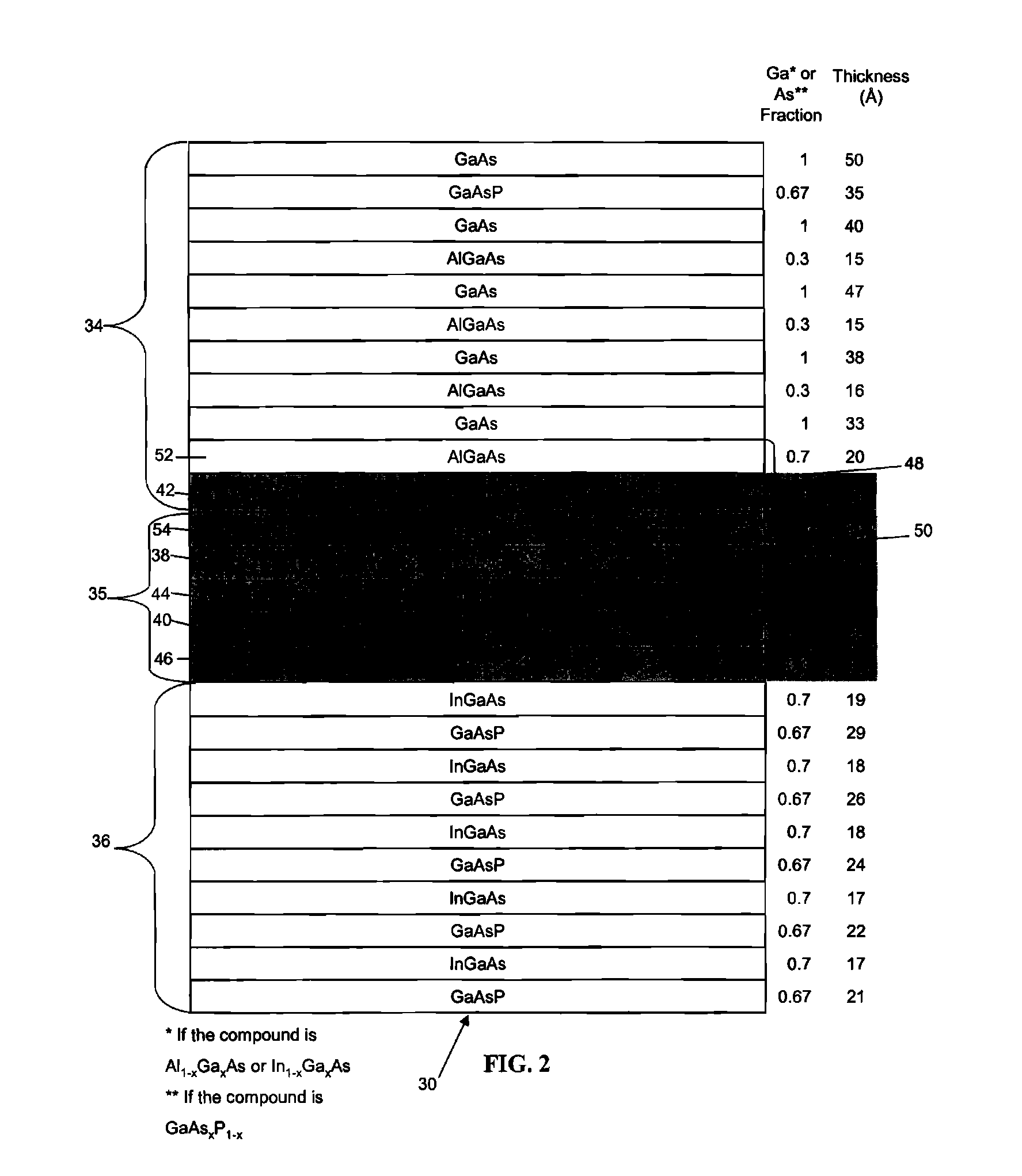
[0034] With reference to the drawings, an example of an implementation of the intersubband quantum cascade laser of the present invention is illustrated generally at 20 in FIG. 1, a simplified cross-sectional view through the multi-layer semiconductor structure. For purposes of illustration, the semiconductor laser structure 20 is shown with a top electrode layer 21 and a bottom electrode layer 22, both of which may be formed on the outer faces of the semiconductor structure of, e.g., conducting metal such as aluminum, gold, etc. The structure further includes top and bottom cladding layers 24 and 25, respectively, for example, formed of n-type semiconductor, Adjacent the layers 24 and 25 are semiconductor layers 27 and 28, respectively, which are selected to provide appropriate electrical conduction across them and to have an appropriate index of refraction so as to cooperate with the layers 24 and 25 to provide optical confinement of the emitted light to the region between the lay...


PUM


Abstract

An intersubband quantum cascade laser structure includes multiple coupled laser stages, wherein each stage has a multilayer structure including an electron injector, an active region with at least one quantum well, and an electron reflector. Electrons injected from the injector into the active region at a high energy level relax to a lower energy level with the emission of a photon at, for example, mid-infrared wavelengths. The reflector reflects electrons at the higher energy level at which they were injected and transmits electrons from the lower energy level after emission of a photon. Multiple layers of semiconductor are formed on each side of the multistage structure to provide conduction across the device and to provide optical confinement of the photons emitted.

Description

FIELD OF THE INVENTION [0001] This invention pertains generally to the field of semiconductor lasers and, particularly, to quantum cascade lasers. BACKGROUND OF THE INVENTION [0002] Semiconductor lasers are formed of multiple layers of semiconductor materials. The conventional semiconductor diode laser typically includes an n-type layer, a p-type layer and an undoped layered active structure between them such that when the diode is forward biased electrons and holes recombine within the active structure with the resulting emission of light. The layers adjacent to the active structure typically have a lower index of refraction than the active structure and form cladding layers that confine the emitted light to the active structure and sometimes to adjacent layers. Semiconductor lasers may be constructed to be either edge-emitting or surface-emitting. [0003] A semiconductor laser that emits photons as electrons from within a given quantized energy band, wherein the electrons relax wit...

Claims


Application Information

Patent Timeline
IPC IPC(8): H01S5/00
CPCH01S5/3402B82Y20/00H01S5/3406H01S5/3407Y10S977/951
Inventor BOTEZ, DANXU, DAPENG P.MAWST, LUKE J.
Owner WISCONSIN ALUMNI RES FOUND
Why Eureka
Try Eureka