Electroluminescent device including an anthracene derivative

an anthracene and el technology, applied in the direction of organic semiconductor devices, discharge tube luminescnet screens, natural mineral layered products, etc., can solve the problems of poor stability, many undesirable applications, and the performance limitations of anthracenes described previously, so as to improve the emission efficiency and stability, improve the oled properties, and improve the drive voltage

Inactive Publication Date: 2007-11-01
GLOBAL OLED TECH
View PDF8 Cites 11 Cited by
  • Summary
  • Abstract
  • Description
  • Claims
  • Application Information

AI Technical Summary

Benefits of technology

[0020] The invention provides improved OLED properties such as improved drive voltage, emission efficiency and stability.

Problems solved by technology

While organic electroluminescent (EL) devices have been known for over two decades, their performance limitations have represented a barrier to many desirable applications.
The phenyl group is substituted in the ortho-position with an aryl group, however materials of this type, when used in EL devices, may result in poor stability.
However, anthracenes that have been described previously may not provide all the desirable embodiments of a host material.

Method used


Image

  • Electroluminescent device including an anthracene derivative
  • Electroluminescent device including an anthracene derivative
  • Electroluminescent device including an anthracene derivative

Examples


example 1

Preparation of Inv-12.

[0187] 9,10-Dibromo-2-chloroanthracene was prepared by the following procedure. 2-Chloroanthracene (5g, 23.5 mmol, 1eq) was suspended in 100 mL of methylene chloride, followed by the addition of N-bromosuccinimide (8.36 g, 47 mmol, 2.0 eq). The slurry was stirred at room temperature, after 1 h only a trace of monobromo material was detected by thin layer chromatography analysis. The flask was heated in a warm water bath. Within a few minutes, the solution cleared and turned orange, followed by the precipitation of yellow solid. Stirring became difficult, therefore an additional portion of 50 mL of methylene chloride was added, and the mixture was stirred at room temperature for an additional hour, to completion. The yellow precipitate was isolated by filtration, and the solid cake washed with acetonitrile. During filtration, more solid had precipitated out in the filtering flask. A second crop of solid was isolated by filtration and combined with the first cro...

example 2

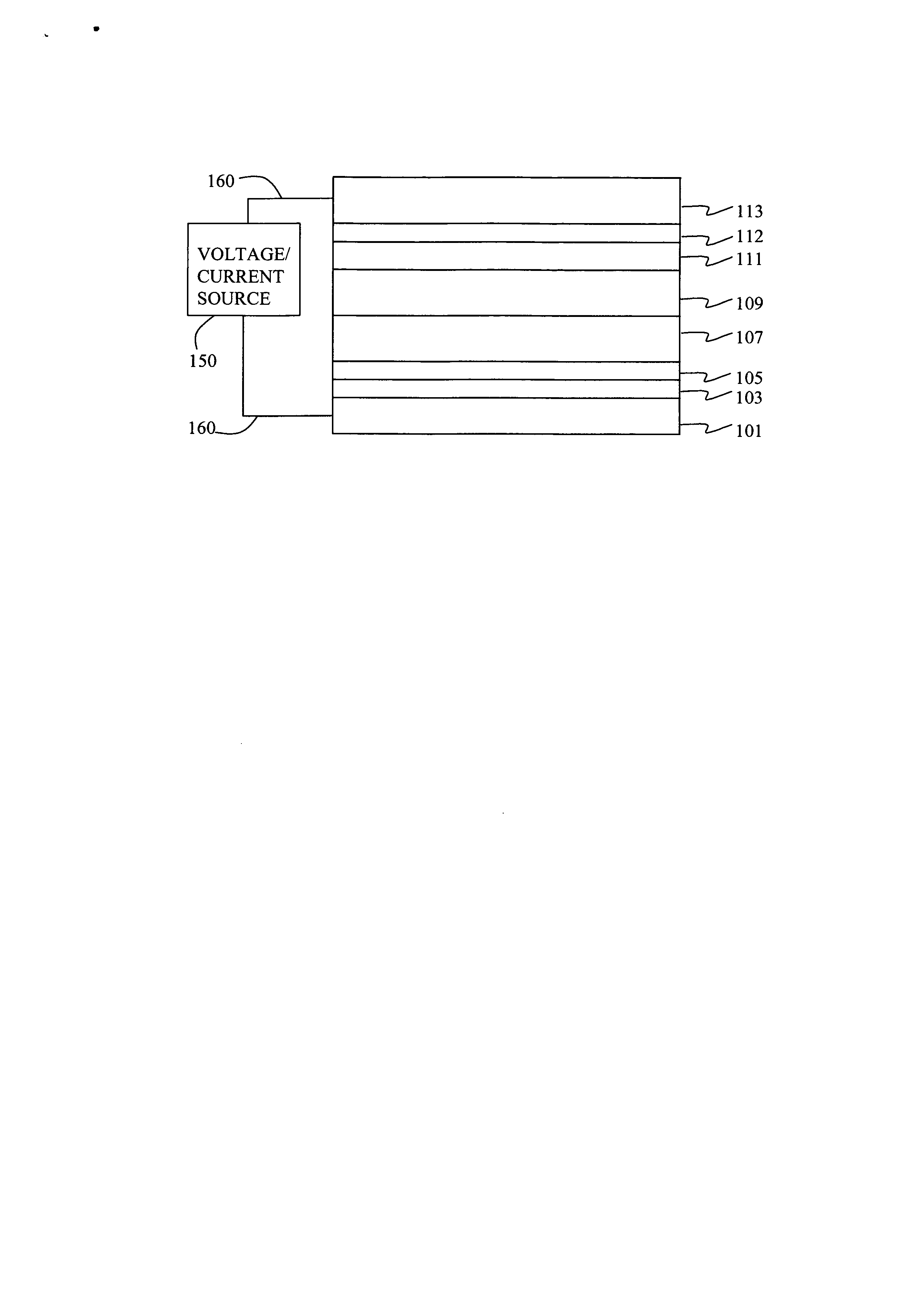
Fabrication of Device 1-1 through 1-6.

[0189] A series of EL devices (1-1 through 1-6) were constructed in the following manner. [0190] 1. A glass substrate coated with a 25 nm layer of indium-tin oxide (ITO), as the anode, was sequentially ultrasonicated in a commercial detergent, rinsed in deionized water, degreased in toluene vapor and exposed to oxygen plasma for about 1 min. [0191] 2. Over the ITO was deposited a 1 nm fluorocarbon (CFx) hole-injecting layer (HIL) by plasma-assisted deposition of CHF3 as described in U.S. Pat. No. 6,208,075. [0192] 3. Next a layer of hole-transporting material 4,4′-Bis[N-(l -naphthyl)-N-phenylamino]biphenyl (NPB) was deposited to a thickness of 75 nm. [0193] 4. A light-emitting layer (LEL) at a thickness shown in Table 1a and corresponding to C-1 or Inv-1 (see Table 1a) and including light-emitting material, (D-1), at the level shown in Table 1a was then deposited. [0194] 5. An electron-transporting layer (ETL) of tris(8-quinolinolato)aluminum (...

example 3

Fabrication of Device 2-1 through 2-6.

[0201] A series of EL devices (2-1 through 2-6) were constructed in the same manner as devices 1-1 through 1-6 except the LEL host was C-1 or Inv-2 (see Table 2a). The LEL emitter (D-1) level, the thickness of the LEL, as well as the ETL thickness are also shown in Table 2a.

[0202] The devices were tested for luminous efficiency and color at an operating current of 20 mA / cm2 and the results are reported in Table 2b in the 5 form of luminous yield (cd / A), efficiency (w / A) and 1931 CIE coordinates. Drive voltage is reported in volts.

[0203] Device stability was determined by operating the device (40 mA / cm2) at ambient temperature for 350 hours. The percent luminance remaining after 350 hours relative to the initial luminance is listed in Table 2b.

TABLE 2aLEL and ETL for Devices 2-1 through 2-6.LELEmitterETLLELThick.LevelThick.ExampleHost(nm)(%)(nm)2-1ComparativeC-1300.75252-2InventiveInv-2200.75352-3InventiveInv-2300.75252-4InventiveInv-2400.75...


PUM

PropertyMeasurementUnit
thickaaaaaaaaaa
operating voltagesaaaaaaaaaa
wavelength rangeaaaaaaaaaa

Abstract

An OLED device comprises a cathode, an anode, and has therebetween a light emitting layer (LEL), at least one layer between the cathode and anode comprising a carbocyclic 2-aryl-9,10-biphenylanthracene compound containing a total of 8-12 aromatic rings, wherein the 6-substituent is hydrogen or an alkyl group and the 2-substituent is: (A) an unsubstituted phenyl group; (B) a phenyl group substituted with (a) a fluoro, a cyano, or an alkyl group or (b) a m- or p-phenyl group; or (C) a substituted or unsubstituted fused ring aromatic group.

Description

CROSS-REFERENCE TO RELATED APPLICATIONS [0001] This application is cofiled as part of a group of five applications under attorney Docket Nos. 91082, 91926, 92030, 92055, and 92056. FIELD OF THE INVENTION [0002] This invention relates to an electroluminescent (EL) device comprising a light-emitting layer and including at least one layer containing an anthracene derivative that can provide desirable electroluminescent properties. BACKGROUND OF THE INVENTION [0003] While organic electroluminescent (EL) devices have been known for over two decades, their performance limitations have represented a barrier to many desirable applications. In simplest form, an organic EL device is comprised of an anode for hole injection, a cathode for electron injection, and an organic medium sandwiched between these electrodes to support charge recombination that yields emission of light. These devices are also commonly referred to as organic light-emitting diodes, or OLEDs. Representative of earlier orga...

Claims


Application Information

Patent Timeline
Patent Type & Authority Applications(United States)
IPC IPC(8): H01L51/54
CPCC09K11/06H05B33/20C09K2211/1014C09K2211/1029C09K2211/1033C09K2211/1037C09K2211/104C09K2211/1044C09K2211/1055C09K2211/107C09K2211/1074C09K2211/1088C09K2211/185H01L51/0052H01L51/0058H01L51/0059H01L51/0062H01L51/008H01L51/5012H01L2251/308H05B33/14C09K2211/1011H10K85/615H10K85/631H10K85/626H10K85/649H10K85/322H10K50/11H10K2102/103
Inventor COSIMBESCU, LELIACONLEY, SCOTT R.OWCZARCZYK, ZBYSLAW R.
Owner GLOBAL OLED TECH
Why Eureka
Try Eureka