Semiconductor device embedded with pressure sensor and manufacturing method thereof

a semiconductor device and sensor technology, applied in the direction of fluid pressure measurement, fluid pressure measurement by electric/magnetic elements, instruments, etc., can solve the problems of many manufacturing limitations, difficult limitation of capacitor area reduction, etc., to achieve significant reduction of chip area of semiconductor devices embedded with pressure sensors, low power consumption, and manufacturing significantly easy

Active Publication Date: 2007-11-15
HITACHI LTD
View PDF3 Cites 31 Cited by
  • Summary
  • Abstract
  • Description
  • Claims
  • Application Information

AI Technical Summary

Benefits of technology

[0017] In the semiconductor device embedded with pressure sensor disclosed in Patent Document 3 and Non-patent Documents 3 to 5, because of the above-described structure, the sensor area and the semiconductor device area are completely separated on the substrate. Therefore, the chip area amounts to a total of the semiconductor device area and the capacitor area. Moreover, as described in Non-patent Documents 2 to 5, in order to perform highly accurate measurement with a capacitive pressure sensor, in addition to a capacitor for measurement, a reference capacitor serving as a reference of pressure and having the same structure is required. Although microfabrication of a semiconductor device can reduce the area occupied by the semiconductor device, the capacitance of these capacitors has to be large to some extent for highly accurate detection of pressure. Thus, the reduction in capacitor area has a limitation. As the semiconductor device is more microfabricated, the ratio of the area occupied by the capacitors in the chip increases. The existence of the capacitor area becomes a large restriction on reduction in chip area, thereby inhibiting the cost reduction of the semiconductor device embedded with pressure sensor.
[0034] Since a semiconductor device can be formed on a layer located lower than a pressure detecting unit, the chip area of the semiconductor device embedded with pressure sensor can be reduced. In particular, when a pressure detecting unit using a pressure-sensitive conductive film is applied, unlike a capacitance type, it is enough to connect two or more electrodes from only the lower layers of the pressure detecting unit to the pressure-sensitive conductive film. This is advantageous in that a semiconductor device embedded with pressure sensor can be manufactured significantly easily. Also, other than the application and change of a planarization process to be performed according to need, no influence is exerted on semiconductor devices located lower than the pressure detecting unit. Therefore, no limitation occurs on the semiconductor device manufacturing method. Consequently, it is possible to embed a highly-microfabricated high-performance semiconductor device and a pressure sensor, and as a result, the low power consumption can be achieved. Furthermore, since the pressure detecting unit is formed on an upper layer of a semiconductor device and the semiconductor device is protected by a nitride film or a polyimide film, it becomes possible to simplify the packaging more than that in the conventional technologies.

Problems solved by technology

Even so, there are many manufacturing limitations.
The largest problem is that the reduction of a chip area of the semiconductor device embedded with pressure sensor is difficult.
Thus, the reduction in capacitor area has a limitation.
Other than the above-described chip-area problem, the conventional technologies have manufacturing limitations.
A large internal stress may cause the characteristic of the diaphragm to be varied with time or may cause the life of the diagraph to be reduced.
Since the heat treatment for releasing the stress is performed at high temperatures, there is a problem that the transistor characteristic is deteriorated if this heat treatment process is inserted after the transistor is formed.

Method used


Image

  • Semiconductor device embedded with pressure sensor and manufacturing method thereof
  • Semiconductor device embedded with pressure sensor and manufacturing method thereof
  • Semiconductor device embedded with pressure sensor and manufacturing method thereof

Examples


first embodiment

[0076] In the first embodiment, the present invention is applied to a semiconductor device embedded with pressure sensor in which a digital circuit, an analog circuit such as an amplifier for amplifying a sensor signal and a wireless transceiver circuit, a flash memory circuit of a MONOS (Metal Oxide Nitride Oxide) type, a capacitive pressure sensor and the like are embedded together on one chip.

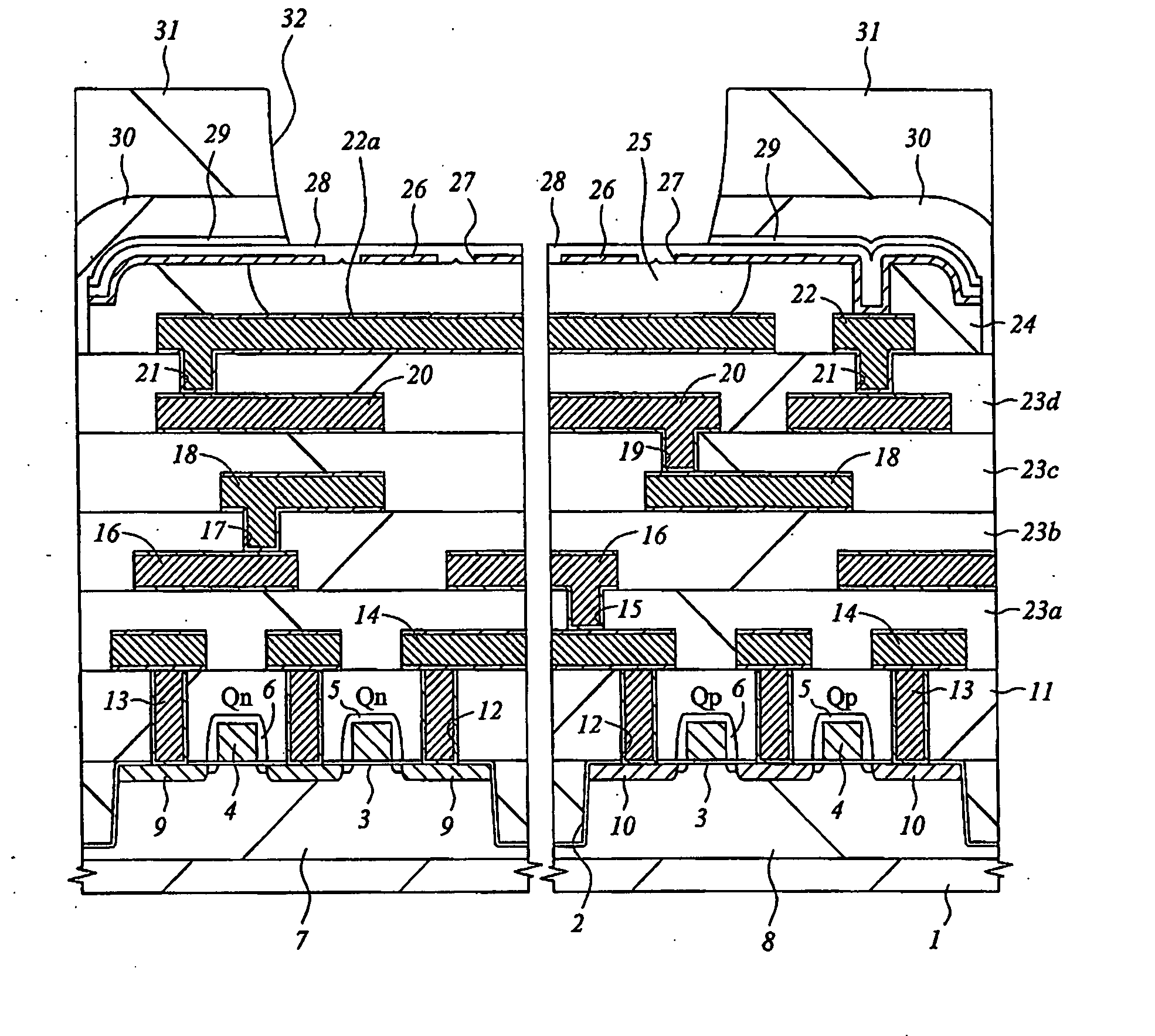
[0077]FIG. 1 is a section view of main components including a pressure detecting unit of a semiconductor device embedded with pressure sensor according to the first embodiment. On the surface of a silicon substrate 1, a trench isolation 2 is formed, and MOS (Metal Oxide semiconductor) transistors (Qn, Qp) having a gate oxide film 3, a gate electrode 4 formed of a polycide film, a cap insulating film 5, a side wall 6, and others are formed. The n channel type MOS transistor (Qn) is formed on a p type well 7, and the p channel type MOS transistor (Qp) is formed on an n type well 8. The minimu...

second embodiment

[0134] In the second embodiment, the present invention is applied to a semiconductor device embedded with pressure sensor in which a digital circuit, an analog circuit such as an amplifier for amplifying a sensor signal and a wireless transceiver circuit, a flash memory circuit of a MONOS type, a capacitive pressure sensor and the like are embedded together on one chip.

[0135] As shown in FIG. 29, the silicon oxide film 24 on the fifth layer wiring 22, which is the uppermost layer wiring, and the lower electrode 22a is planarized by CMP so as to have a height equal to that of the fifth layer wiring 22 and the lower electrode 22a. On the upper portion of the silicon oxide film 24, the fifth layer wiring 22, and the lower electrode 22a, a silicon oxide film 47 is formed, and the diaphragm is formed thereon. The cavity 25 under the diaphragm is filled with gas containing nitrogen as the main component at atmospheric pressure, and a silicon dioxide film 46 is formed on the inner wall th...

third embodiment

[0143] In the third embodiment, the present invention is applied to a semiconductor device embedded with pressure sensor in which a digital circuit, an analog circuit such as an amplifier for amplifying a sensor signal and a wireless transceiver circuit, an EEPROM circuit, a capacitive pressure sensor and the like are embedded together on one chip.

[0144] A method of manufacturing a pressure detecting unit according to this embodiment will be described with reference to FIG. 33 to FIG. 37. First, the first layer wiring 14 to the fifth layer wiring 22 and the lower electrode 22a are formed on the silicon substrate 1 in the same manner as that of the above-described first embodiment, and then, as shown in FIG. 33, a silicon nitride film 53 on the silicon substrate 1 is patterned so that the patterned silicon nitride film 53 is left on the upper portion and the periphery of the lower electrode 22a. Then, a silicon oxide film 54 is deposited on the silicon substrate 1, and the surface o...


PUM

PropertyMeasurementUnit
timeaaaaaaaaaa
heat treatment temperatureaaaaaaaaaa
gate lengthaaaaaaaaaa

Abstract

The method for promoting the size reduction, the performance improvement and the reliability improvement of a semiconductor device embedded with pressure sensor is provided. In a semiconductor device embedded with pressure sensor, a part of an uppermost wiring is used as a lower electrode of a pressure detecting unit. A part of a silicon oxide film formed on the lower electrode is a cavity. On a tungsten silicide film formed on the silicon oxide film, a silicon nitride film is formed. The silicon nitride film has a function to fill a hole or holes and suppress immersion of moisture from outside to the semiconductor device embedded with pressure sensor. A laminated film of the silicon nitride film and the tungsten silicide film forms a diaphragm of the pressure sensor.

Description

CROSS-REFERENCE RELATED APPLICATION [0001] This application is a Continuation of nonprovisional U.S. application Ser. No. 11 / 237,897 filed on Sep. 29, 2005. Priority is claimed based on U.S. application Ser. No. 11 / 237,897 filed on Sep. 29, 2005, which claims priority from Japanese Patent Applications 2004-289476 filed on Oct. 1, 2004 and 2005-284013 filed on Sep. 29, 2005, the contents of which are hereby incorporated by reference into this application.TECHNICAL FIELD OF THE INVENTION [0002] The present invention relates to a semiconductor device embedded with pressure sensor and a manufacturing method thereof. More particularly, the present invention relates to a technology effectively applied to the size reduction of a semiconductor device embedded with pressure sensor and the performance enhancement thereof. BACKGROUND OF THE INVENTION [0003] Pressure sensors are sensors used in various fields. Of these, the demands for a small-sized pressure sensor formed by using MEMS (Micro E...

Claims


Application Information

Patent Timeline
Patent Type & Authority Applications(United States)
IPC IPC(8): H01L29/84
CPCG01L9/0073H01L2224/32245H01L2224/48247H01L2224/73265H01L2924/181H01L2924/00012H01L2924/00
Inventor YOKOYAMA, NATSUKIMACHIDA, SHUNTAROGOTO, YASUSHI
Owner HITACHI LTD
Why Eureka
Try Eureka