Circuit configurations to reduce snapback of a transient voltage suppressor

a transient voltage and suppressor technology, applied in the field of circuit configuration and method of manufacture of transient voltage suppressors, can solve the problems of large area to reduce resistance, circuit damage, unexpected and uncontrollable high voltage hitting the circuit, etc., to improve clamping, reduce voltage drop, and increase break down voltage

Active Publication Date: 2007-12-06
ALPHA & OMEGA SEMICON LTD
View PDF4 Cites 43 Cited by
  • Summary
  • Abstract
  • Description
  • Claims
  • Application Information

AI Technical Summary

Benefits of technology

[0008]It is therefore an aspect of the present invention to provide an improved TVS circuit to have an improved clamping. It is therefore a further aspect of the present invention to provide an improved TVS circuit to reduce the voltage-drop in a reverse-blocking voltage snap-back when a reverse current transmi

Problems solved by technology

However, in situations such as electrostatic discharge (ESD), electrical fast transients and lightning, an unexpected and an uncontrollable high voltage may accidentally strike onto the circuit.
Since the Zener diode has higher resistance per unit area compared with BJT or SCR and BJT this is actually a disadvantage at higher currents because the steering diodes also have to be rugged in reverse conduction.
The problem with the Vcc−Gnd clamp diodes is that typically these diodes are very resistive in reverse blocking mode and require large ar

Method used


Image

  • Circuit configurations to reduce snapback of a transient voltage suppressor
  • Circuit configurations to reduce snapback of a transient voltage suppressor
  • Circuit configurations to reduce snapback of a transient voltage suppressor

Examples


Embodiment Construction

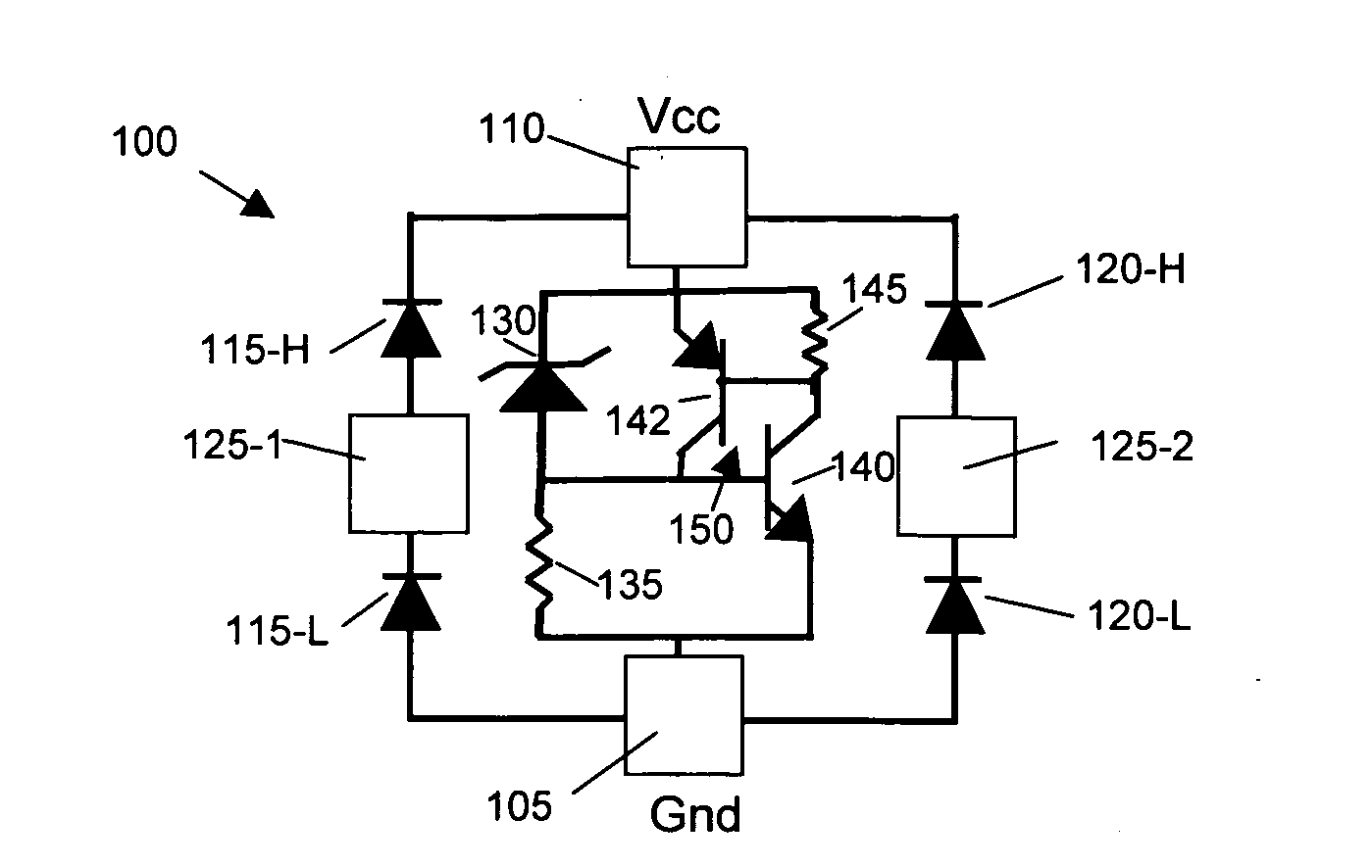
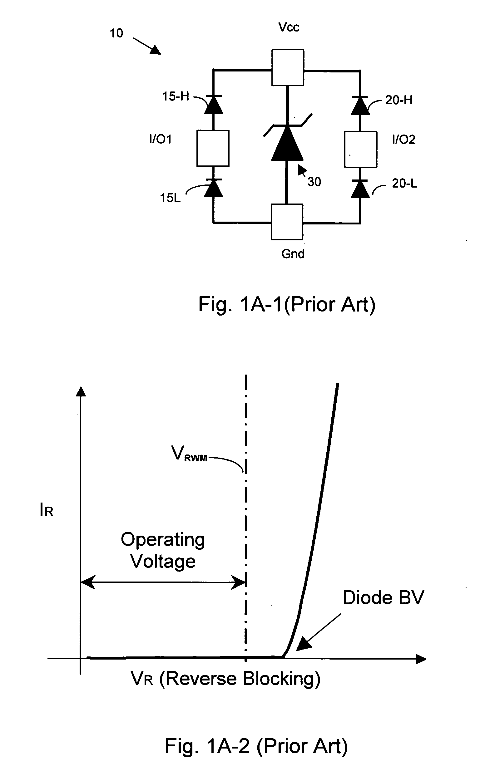
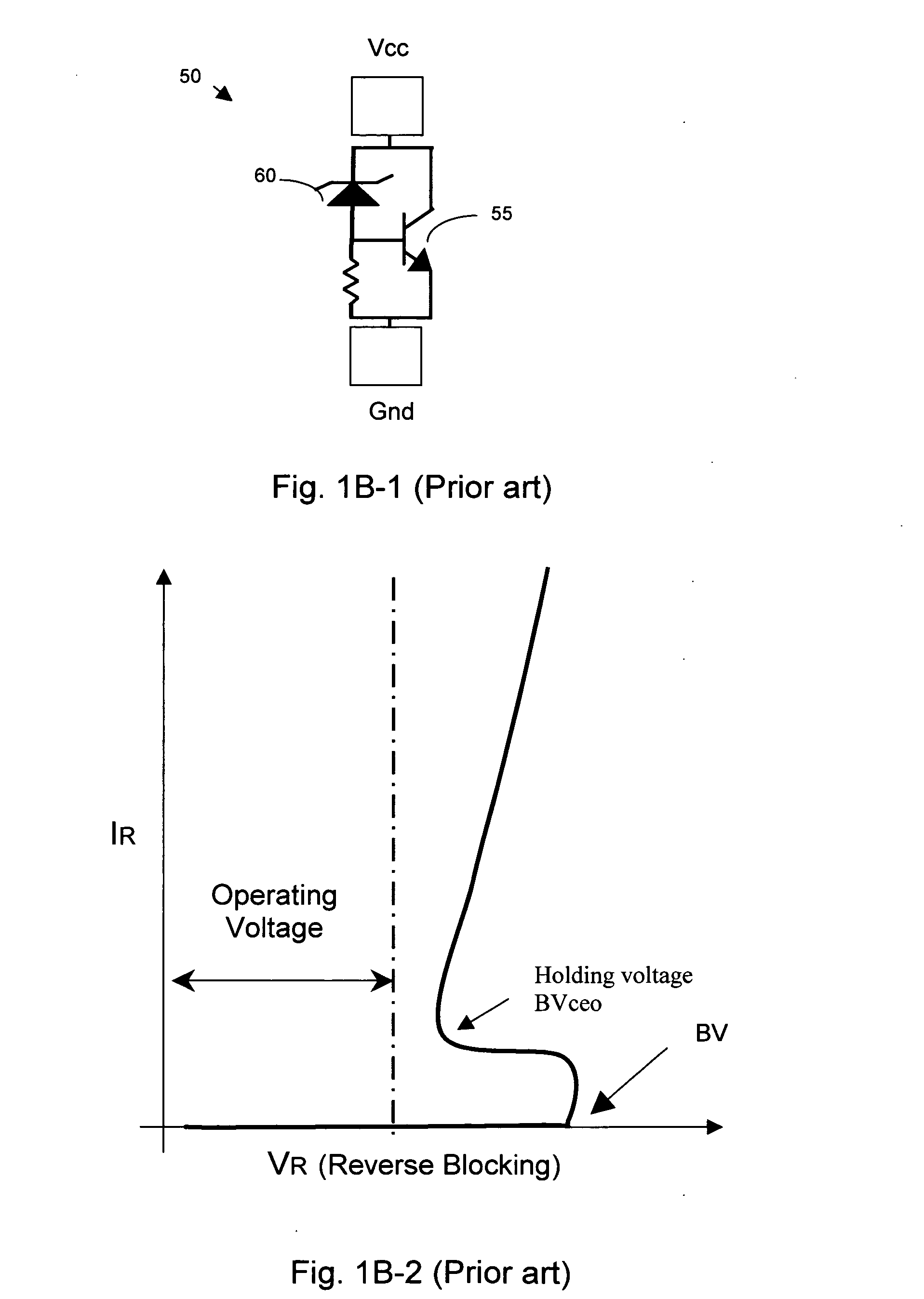
[0021]Referring to FIGS. 2A and 2B for a circuit diagram and an I-V diagram, i.e., a current versus voltage diagram, respectively of a TVS circuit 100 of this invention. The TVS circuit 100 is installed between a ground voltage terminal (Gnd) 105 and a Vcc voltage terminal 110 to function as a Vcc-Gnd clamp circuit. The TVS circuit 100 includes two sets of steering diodes, i.e., diodes 115-H and 115-L and 120-H and 120-L respectively for each of the two input / output (I / Os) terminals 125-1 and 125-2. Furthermore, there is a Zener diode, i.e., diode 130, with a larger size to function as an avalanche diode from the high voltage terminal, i.e., terminal Vcc, to the ground voltage terminal, i.e., terminal Gnd. The Zener diode 130 is connected in series with a resistor 135 and in parallel to a NPN bipolar transistor 140. A PNP bipolar transistor 142 in configured with NPN bipolar transistor 140 forms a PNPN silicon-controlled rectifier (SCR) structure 150 with high holding current and vo...


PUM


Abstract

This invention discloses an electronic device formed as an integrated circuit (IC) wherein the electronic device further includes a transient voltage suppressing (TVS) circuit. The TVS circuit includes a triggering Zener diode connected between an emitter and a collector of a bipolar-junction transistor (BJT) wherein the Zener diode having a reverse breakdown voltage BV less than or equal to a BVceo of the BJT where BVceo stands for a collector to emitter breakdown voltage with base left open. The TVS circuit further includes a rectifier connected in parallel to the BJT for triggering a rectified current through the rectifier for further limiting an increase of a reverse blocking voltage. In a preferred embodiment, the triggering Zener diode, the BJT and the rectifier are formed in a semiconductor substrate by implanting and configuring dopant regions of a first and a second conductivity types in a N-well and a P-well whereby the TVS can be formed in parallel as part of the manufacturing processes of the electronic device.

Description

BACKGROUND OF THE INVENTION[0001]1. Field of the Invention[0002]The invention relates generally to a circuit configuration and method of manufacture of a transient voltage suppressor (TVS). More particularly, this invention relates to an improved circuit configuration and method of manufacture of a transient voltage suppressor (TVS) with greatly reduced snapback.[0003]2. Description of the Relevant Art[0004]The transient voltage suppressors (TVS) are commonly applied for protecting integrated circuits from damages due to the inadvertent occurrence of an over voltage imposed onto the integrated circuit. An integrated circuit is designed to operate over a normal range of voltages. However, in situations such as electrostatic discharge (ESD), electrical fast transients and lightning, an unexpected and an uncontrollable high voltage may accidentally strike onto the circuit. The TVS devices are required to serve the protection functions to circumvent the damages that are likely to occur ...

Claims


Application Information

Patent Timeline
IPC IPC(8): H02H9/06
CPCH01L29/87H01L27/0262H01L27/02H01L29/861
Inventor MALLIKARARJUNASWAMY, SHEKAR
Owner ALPHA & OMEGA SEMICON LTD
Why Eureka
Try Eureka