
Solderable pads utilizing nickel and silver nanoparticle ink jet inks

Inactive Publication Date: 2007-12-06
CABOT CORP
View PDF10 Cites 29 Cited by
  • Summary
  • Abstract
  • Description
  • Claims
  • Application Information

AI Technical Summary

Benefits of technology

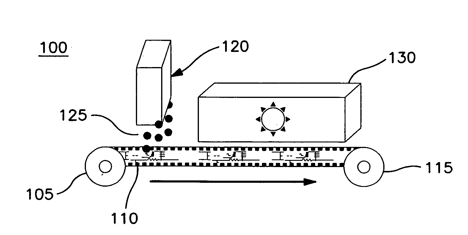
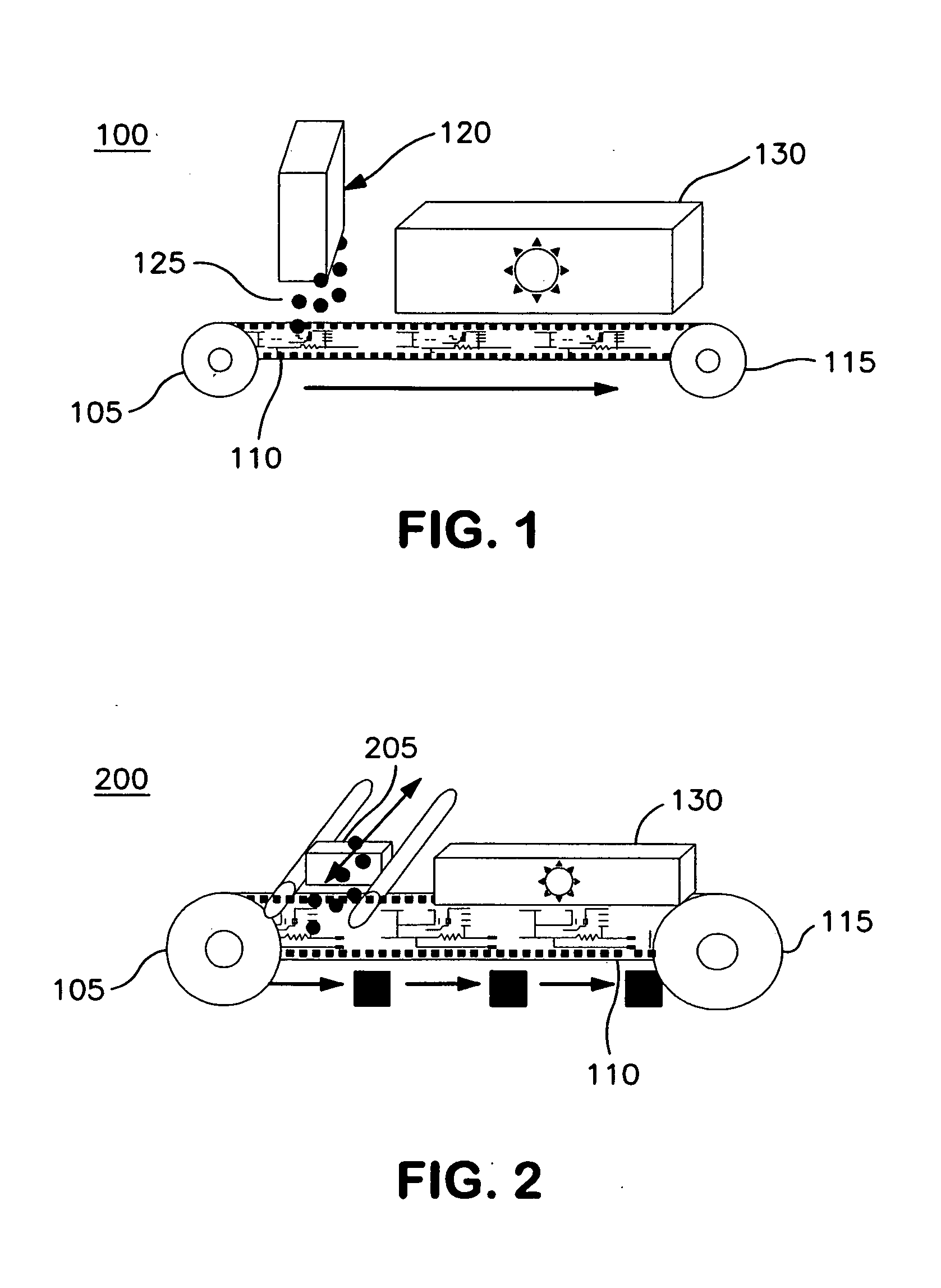
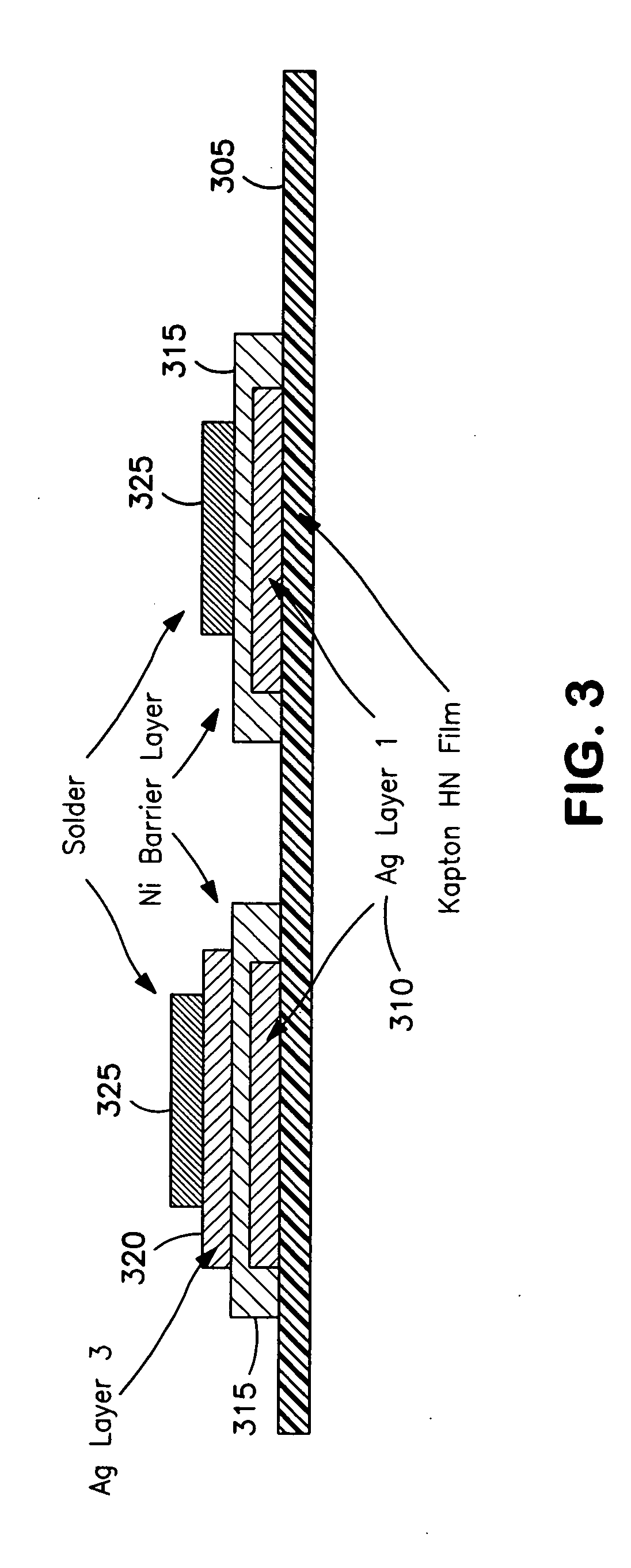
[0011]In one aspect, the invention provides an ink-jet printing system for printing a solderable conductive pad onto a substrate. The system comprises at least one print head and a curing station for curing an ink deposited onto the substrate. The system is configured to: deposit at least a first layer of a first ink onto the substrate; cure the first layer of the first ink; deposit at least an intermediate layer of a second ink on top of the cured first layer of the first ink; cure the intermediate layer of the second ink; deposit at least a last layer of the first ink on top of the cured intermediate layer of the second ink; and cure the last layer of the first ink. The first ink has a relatively high conductivity. The second ink has a relatively low conductivity. The first layer, the intermediate layer, and the last layer may be arranged such that when solder is applied to the last layer, the solder is prevented from leaching through to the first layer.
[0014]In another aspect, the invention provides a process for ink-jet printing a solderable conductive pad onto a substrate. The process comprises the steps of: depositing a first layer of a first ink onto the substrate; curing the deposited first layer; depositing an intermediate layer of a second ink on top of the cured first layer; curing the deposited intermediate layer; depositing a last layer of the first ink on top of the cured intermediate layer; and curing the deposited last layer. The first ink has a relatively high conductivity. The second ink has a relatively low conductivity. The first layer, the intermediate layer, and the last layer may be arranged such that when solder is applied to the last layer, the solder is prevented from leaching through to the first layer.

Problems solved by technology

There are a number of deficiencies inherent in this process using solder masks.
This is wasteful of materials.
The phototool is distanced from the solder mask film, and because of light diffraction, some areas of the liquid solder mask which are not directly beneath the exposed areas of the phototool may tend to polymerize, and therefore become more difficult to remove using aqueous alkali.
This adversely affects the definition and line density of those parts of the copper circuitry for which it is desired to expose for contact with the solder paste.
Furthermore, use of solder mask acrylate polymers which need to be quickly and effectively removed in a relatively short time frame requires a relatively high carboxylic acid content.
This can have an adverse impact on those parts of the solder mask which are retained for protection of the individual elements of the PCB.
It also eliminates flow problems in applying liquid solder mask to the whole of the dielectric substrate containing the copper circuitry where it is often difficult to avoid entrainment of air between adjacent copper tracks, which can adversely affect PCB performance and longevity.
Such leaching can cause significantly reduced performance of the electrically circuitry.

Method used


Image

  • Solderable pads utilizing nickel and silver nanoparticle ink jet inks
  • Solderable pads utilizing nickel and silver nanoparticle ink jet inks
  • Solderable pads utilizing nickel and silver nanoparticle ink jet inks

Examples


Embodiment Construction

[0022]In one aspect, the invention provides an ink-jet printing system for printing a solderable conductive pad onto a substrate. The system comprises at least one print head and a curing station for curing an ink deposited onto the substrate. The system is configured to: deposit at least a first layer of a first ink onto the substrate; cure the first layer of the first ink; deposit at least an intermediate layer of a second ink on top of the cured first layer of the first ink; cure the intermediate layer of the second ink; deposit at least a last layer of the first ink on top of the cured intermediate layer of the second ink; and cure the last layer of the first ink. The first ink has a relatively high conductivity. The second ink has a relatively low conductivity. The first layer, the intermediate layer, and the last layer may be arranged such that when solder is applied to the last layer, the solder is prevented from leaching through to the first layer.

[0023]The first ink may com...


PUM

PropertyMeasurementUnit
Thicknessaaaaaaaaaa
Thicknessaaaaaaaaaa
Thicknessaaaaaaaaaa

Abstract

A system and a method are provided for ink-jet printing a solderable conductive pad onto a substrate. The system comprises at least one print head and a curing station for curing an ink deposited onto the substrate. The system is configured to: deposit at least a first layer of a first ink onto the substrate; cure the first layer of the first ink; deposit at least an intermediate layer of a second ink on top of the cured first layer of the first ink; cure the intermediate layer of the second ink; deposit at least a last layer of the first ink on top of the cured intermediate layer of the second ink; and cure the last layer of the first ink. The first ink has a relatively high conductivity. The second ink has a relatively low conductivity. The first layer, the intermediate layer, and the last layer may be arranged such that when solder is applied to the last layer, the solder is prevented from leaching through to the first layer.

Description

BACKGROUND OF THE INVENTION[0001]1. Field of the Invention[0002]The present invention relates to ink-jet printing of electrical components onto a substrate using conductive inks. More particularly, the invention relates to a method and apparatus for printing solderable pads onto a substrate using layers of inks that are selected to prevent leaching of solder through to the base ink layer.[0003]2. Related Art[0004]In the conventional manufacture of printed circuit boards (PCBs), a laminate comprising a dielectric substrate having a copper sheet affixed to at least one side is prepared. The copper surface is overlaid with a photo-resist layer which is typically a carboxylic acid containing polyacrylate. A phototool is prepared which is a negative image of the desired copper electrically conductive circuitry, and this is typically a silver halide photographic emulsion. The phototool is placed over the photo-resist layer and irradiated with actinic radiation, such as ultraviolet (UV) li...

Claims


Application Information

Patent Timeline
IPC IPC(8): B05D1/12B05D3/02B05D7/00B05C5/00B41J2/01
CPCH05K1/095H05K3/125H05K3/247H05K2203/1476H05K2201/035H05K2203/013H05K2201/0257
Inventor HOWARTH, JAMES J.JAMES, ANTHONY R.VANHEUSDEN, KAREL
Owner CABOT CORP
Learn More