Method and apparatus for detecting defect on a surface of a specimen

a surface inspection and specimen technology, applied in the direction of interferometers, instruments, material analysis, etc., can solve the problems of difficult to perform entire surface inspection, difficult to detect defects on the surface, and failure of hard disk drives, so as to improve surface recording density, reduce surface roughness, and reduce the size of hard disk drives

Inactive Publication Date: 2007-12-13
HITACHI HIGH-TECH CORP
View PDF13 Cites 9 Cited by
  • Summary
  • Abstract
  • Description
  • Claims
  • Application Information

AI Technical Summary

Benefits of technology

[0018] In accordance with the present invention, it is possible to measure the shape of crystal defect, a residual abrasive particle, a fine flaw (scratch or the like), a foreign material, and other minute concavo-convex defects (including surface roughness) on a surface of a disk substrate having a tendency to decreasing surface roughness due to improved surface recording density, decreased size of hard disk drive, etc. based on the interference-phase measurement scheme using a diode laser light source with a large spectrum width having a very short coherence length of several millimeters, thus realizing a method and a low-price simply constructed apparatus for surface inspection.

Problems solved by technology

Therefore, if minute concavo-convex defect exists on the disk substrate, the head comes in contact with the disk substrate which may cause failure of the hard disk drive.
However, since crystal defect, a scratch, etc. are unrepairable, a product with such defect will be handled as a defective one.
In AFM-based measurement, the throughput is remarkably slow and therefore it is not easy to perform entire surface inspection.
Furthermore, this method has some drawbacks: for example, a measurement probe is a consumable; measurement reproducibility fluctuates because of a worn probe, etc.
As the wavelength is shortened, therefore, the structure of the laser light source becomes more complicated resulting in remarkably high price.
For this reason, there arises a subject of increased price of a surface inspection apparatus.
Thus, since the coherence length becomes remarkably shorter with increasing spectrum width, diode laser is not suitable as a light source for the above-mentioned interference optical system.
With this method, a specific wavelength is taken out from the diffraction grating and therefore the output is remarkably reduced and at the same time the arrangement of the diffraction grating is delicate.
There arises a subject of aging as well as a subject that laser beam cannot be taken out because of vibratory effect on the diode laser light source.
Furthermore, since the configuration of the diode laser light source may become complicated, there arises a subject of high price.

Method used


Image

  • Method and apparatus for detecting defect on a surface of a specimen
  • Method and apparatus for detecting defect on a surface of a specimen
  • Method and apparatus for detecting defect on a surface of a specimen

Examples


first embodiment

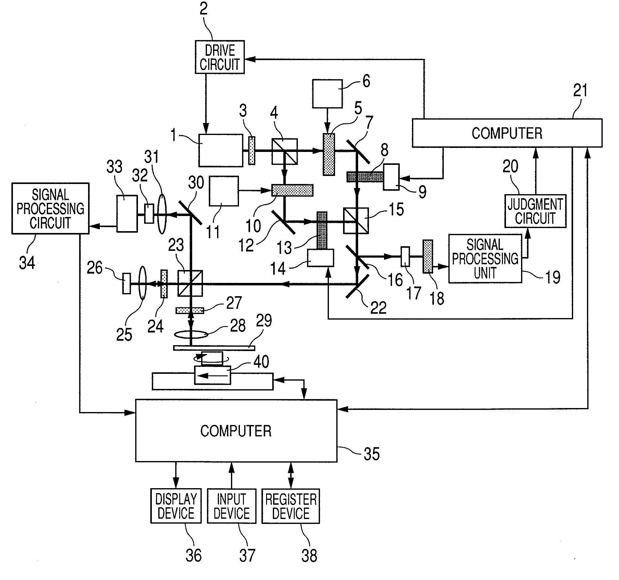
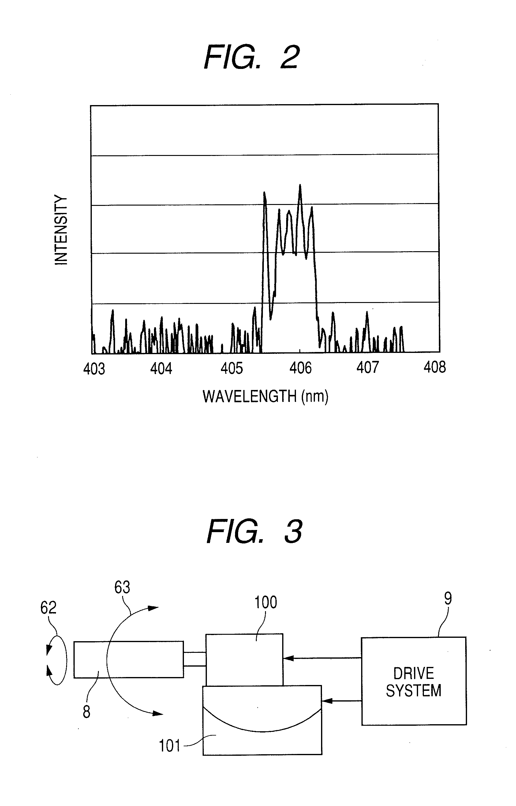
[0034] A first embodiment of a surface inspection method and apparatus of the present invention will be described below with reference to the accompanying drawings. FIG. 2 shows an example of a wide-band spectrum distribution of diode laser of the present invention. Thus, in the case of diode laser, the wavelength is shorter than that of diode-pumped solid state laser (with a wavelength of 532 nm) having a narrow-band spectrum distribution as shown in FIG. 9. However, the spectrum width is several nanometers, generally making it possible to obtain a coherence length of only several millimeters. The present invention is concerned with a surface inspection method and apparatus for measuring the shape of minute concavo-convex defect (including surface roughness) on a surface of a substrate, such as a disk substrate, based on the interference-phase measurement scheme using such wide-band laser.

[0035] A first embodiment of a surface inspection apparatus of the present invention will be ...

second embodiment

[0059] A second embodiment of a surface inspection apparatus of the present invention will be described below with reference to FIG. 13. The second embodiment differs from the first embodiment in that the interference intensity is monitored by the light-sensitive element (the sensor) 33 during inspection. Since at least an interference intensity signal 50 for a flat specimen is also detected by the light-sensitive element 33 as shown in FIG. 5, the interference intensity is measured by the signal processing unit 150 (19); and interference intensity, period, and other information are judged by the judgment circuit 151 (20) and then inputted to the computer 21. If the judgment circuit 151 (20) judges (determines) that the signal has changed to a predetermined interference intensity or lower, it is preferable that the computer 21 activates each of the drive systems 9 and 14 according to the above-mentioned flow chart and adjusts each of the optical path length varying optical elements ...


PUM


Abstract

A surface inspection apparatus is provided based on an optical interference scheme using a wide-band laser light source, such as diode laser, for an interferometer. In the apparatus, a diode laser with a large spectrum width having a short coherence length is used as an emitted light source; modulation optical elements for performing modulation with slightly different frequencies, and optical path length varying optical elements for adjusting the optical path length are located in each of two optical paths between a branching optical element and a combining optical element; and the above-mentioned optical path length varying optical elements are adjusted, while measuring an interference intensity, so as to maximize the interference intensity.

Description

BACKGROUND OF THE INVENTION [0001] 1. Field of the Invention [0002] The present invention relates to a surface inspection apparatus for detecting defect on a surface of a magnetic disk substrate. More particularly, the present invention relates to a surface inspection method and apparatus for measuring the shape of a defect through phase detection. [0003] 2. Description of the Related Art [0004] A disk substrate with evaporated magnetic substance is used as a magnetic recording medium for a hard disk drive. Data is magnetically written and read by magnetizing the disk substrate by use of a magnetic head. In recent years, with an increase in the recording density of hard disk drive, the space (hereinafter referred to as flying height) between a recording head (hereinafter referred to as head) and the disk substrate is becoming much narrower, i.e., from several tens of nanometers to several nanometers. Therefore, if minute concavo-convex defect exists on the disk substrate, the head c...

Claims


Application Information

Patent Timeline
Patent Type & Authority Applications(United States)
IPC IPC(8): G01B9/02
CPCG01B11/2441G01N21/45G01N21/95G01B2290/70G01N2021/95676G01B9/02002G01B9/02067G01N21/9501
Inventor YOSHIDA, MINORUOSHIMA, YOSHIMASA
Owner HITACHI HIGH-TECH CORP
Why Eureka
Try Eureka