Method For Producing Semiconductor Wafer

a technology of semiconductor wafers and semiconductors, applied in the direction of semiconductor devices, basic electric elements, electrical apparatus, etc., can solve the problems of degrading crystallinity, and achieve the effect of suppressing surface roughness and good crystallinity

Inactive Publication Date: 2007-12-13
SHIN-ETSU HANDOTAI CO LTD
View PDF5 Cites 28 Cited by
  • Summary
  • Abstract
  • Description
  • Claims
  • Application Information

AI Technical Summary

Benefits of technology

[0007] An object of the present invention is to provide a method for producing a semiconductor wafer having a SiGe layer in which lattice relaxation is sufficiently performed and of which surface roughness is suppressed and of which crystallinity is good.

Problems solved by technology

However, in the SiGe layer in the SGOI wafer produced by such a conventional method as described above, occasionally, a large number of streak-like irregularities called as crosshatch are generated on the oxidized and enriched surface and surface roughness is caused and also threading dislocations or the like are generated and its crystallinity becomes degraded.

Method used


Image

  • Method For Producing Semiconductor Wafer
  • Method For Producing Semiconductor Wafer
  • Method For Producing Semiconductor Wafer

Examples


example 1

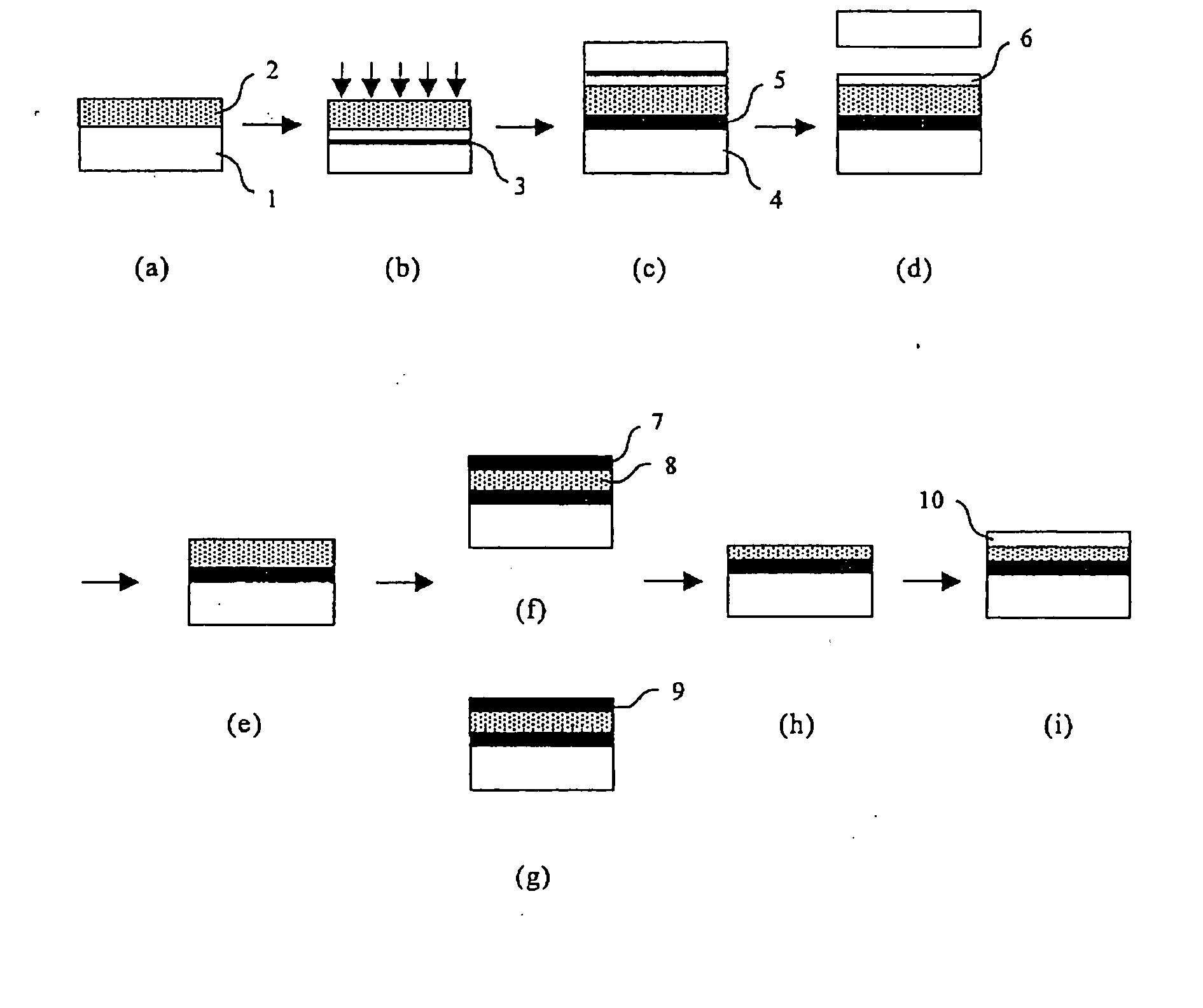
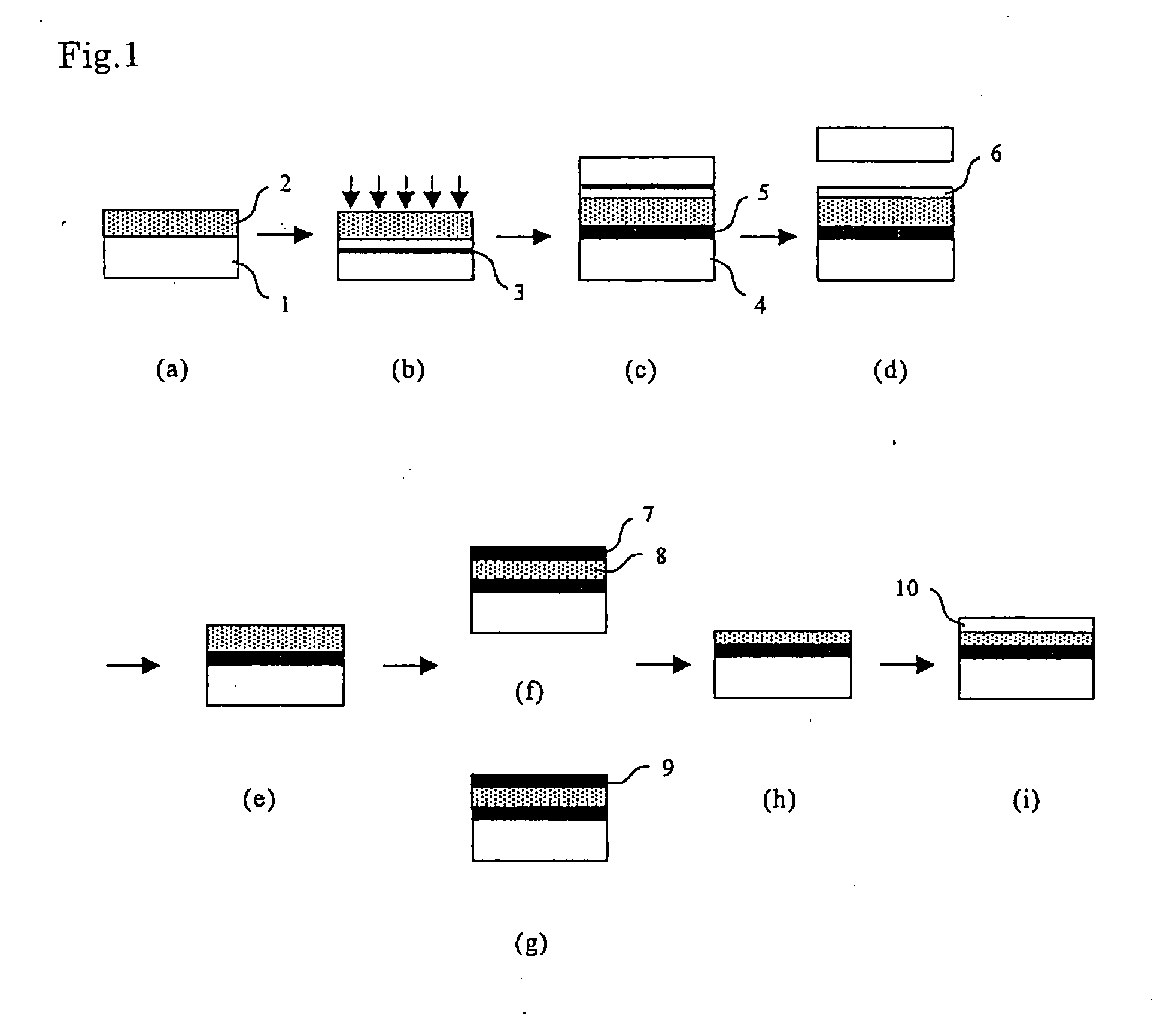
[0082] A SiGe layer (the Ge composition was 10%) was epitaxially grown only at approximately 120 nm by a CVD method, on a surface of a silicon single crystal wafer having a diameter of 200 mm, and through the SiGe layer, hydrogen ion (H+) was ion-implanted under the condition that the implantation energy was 20 keV and the dose amount was 5×10¹⁶ atoms / cm2, and thereby an ion implanted layer was formed inside the silicon single crystal wafer. After the hydrogen ion implantation, the surface of the SiGe layer was cleaned with an SC-1 cleaning solution. This surface and a silicon single crystal base wafer with a thermal oxide film of 100 nm were closely contacted at a room temperature, and delamination heat treatment was performed under an argon atmosphere at 500° C. for 30 min and thereby the delamination was performed at the ion implanted layer. Thereby, the SiGe layer and a part (Si layer) of the silicon single crystal wafer were transferred to a side of the base wafer. Next, the Si...

example 2

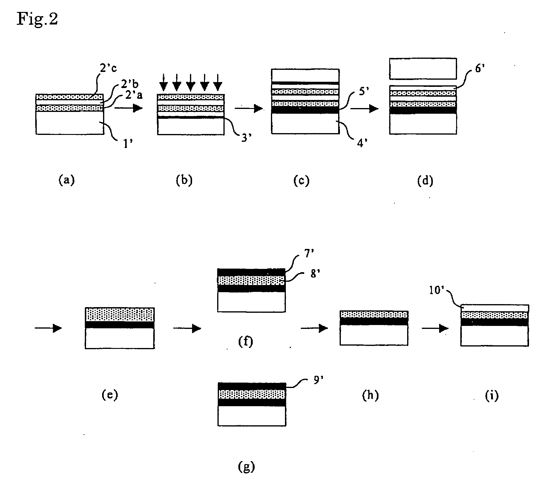
[0084] A SiGe layer (the Ge composition was 20%) of approximately 100 nm, a Si layer of approximately 50 nm, and a SiGe layer (the Ge composition was 20%) of approximately 50 nm were epitaxially grown in order by a CVD method, on a surface of a silicon single crystal wafer having a diameter of 200 mm, and through these epitaxial layers, hydrogen ion (H+) was ion-implanted under the condition that the implantation energy was 20 keV and the dose amount was 5×10¹⁶ atoms / cm2, and thereby an ion implanted layer was formed inside the silicon single crystal wafer. After the hydrogen ion implantation, the surface of the SiGe layer that is the uppermost layer was cleaned with an SC-1 cleaning solution. This surface and a silicon single crystal base wafer with a thermal oxide film of 100 nm were closely contacted at a room temperature, and delamination heat treatment was performed under an argon atmosphere at 500° C. for 30 min and thereby the delamination was performed at the ion implanted l...


PUM


Abstract

The present invention is a method for producing a semiconductor wafer, comprising at least steps of: epitaxially growing a SiGe layer on a surface of a silicon single crystal wafer that is to be a bond wafer; implanting at least one kind of hydrogen ion and rare gas ion through the SiGe layer, so that an ion implanted layer is formed inside the bond wafer; closely contacting and bonding a surface of the SiGe layer and a surface of a base wafer through an insulator film; then performing delamination at the ion implanted layer, removing a Si layer in a delaminated layer transferred to a side of the base wafer by the delamination, so that the SiGe layer is exposed; and then subjecting the exposed SiGe layer to a heat treatment for enriching Ge under an oxidizing atmosphere and/or a heat treatment for relaxing lattice strain under a non-oxidizing atmosphere. Thereby, a method for producing a semiconductor wafer having a SiGe layer in which lattice relaxation is sufficiently performed and of which surface roughness is suppressed and of which crystallinity is good is provided.

Description

TECHNICAL FIELD [0001] The present invention relates to a method for producing a semiconductor wafer having a SiGe layer on an insulator. BACKGROUND ART [0002] In recent years, in order to meet demands for high-speed semiconductor devices, there has been proposed semiconductor devices, such as a high-speed MOSFET (Metal-Oxide-Semiconductor Field Effect Transistor) in which a Si layer that is epitaxially grown on a Si (silicon) substrate through a SiGe (Silicon Germanium) layer is used in a channel region. [0003] In this case, because SiGe crystal has a larger lattice constant than that of Si crystal, tensile strain is being generated in the Si layer that is epitaxially grown on the SiGe layer (hereinafter, such a Si layer in which strain is being generated is called as a strained Si layer). By its strain stress, an energy band structure of the Si crystal is changed and therefore degeneracy of the energy band is dissolved and an energy band with high carrier-mobility is formed. There...

Claims


Application Information

Patent Timeline
Patent Type & Authority Applications(United States)
IPC IPC(8): H01L21/20
CPCH01L21/02381H01L21/0245H01L21/0251H01L21/76254H01L21/0262H01L21/02664H01L21/02532H01L21/20H01L27/12
Inventor YOKOKAWA, ISAONOTO, NOBUHIKO
Owner SHIN-ETSU HANDOTAI CO LTD
Why Eureka
Try Eureka