Curing Dielectric Films Under A Reducing Atmosphere

Inactive Publication Date: 2007-12-27
VERSUM MATERIALS US LLC
View PDF31 Cites 62 Cited by
  • Summary
  • Abstract
  • Description
  • Claims
  • Application Information

AI Technical Summary

Benefits of technology

[0019] The process of the present invention as described below, among other things, efficiently removes at least a portion of the at least one carbon-containing pore-forming material by enhancing the removal of the at least one carbon-containing pore-forming material; decreases the formation of material on the windows and walls

Problems solved by technology

Consequently, various components of IC devices such as Cu metal lines can only be subjected to processing temperatures for short time periods before their performance deteriorates due to undesirable diffusion processes.
These techniques, unfortunately, may adversely affect the resultant film by chemically modifying the bonds that remain within the material.
For example, exposure of these materials to an

Method used


Image

  • Curing Dielectric Films Under A Reducing Atmosphere
  • Curing Dielectric Films Under A Reducing Atmosphere

Examples


Example

Example 1

[0099] Composite films were deposited onto a Si substrate using PE-CVD processing techniques. The composite film was exposed to the UV source as described in Example 1 for 5 minutes. After 5 minutes, the wafer was removed from the chamber and cleaned with oxygen in the presence of UV light for 10 minutes to remove porogen from the window. After purging the chamber with helium, the sample was re-introduced into the chamber and exposed to UV light for an additional 8 minutes under a helium purge (250 sccm He flow rate, chamber pressure of 2 Torr) at 400° C. The chamber was subsequently cleaned with oxygen in the presence of UV light for an additional 5 minutes. The dielectric constant of the film was 2.5, refractive index of 1.36, and an extinction coefficient at 240 nm of 0.032.

Example

Example 2

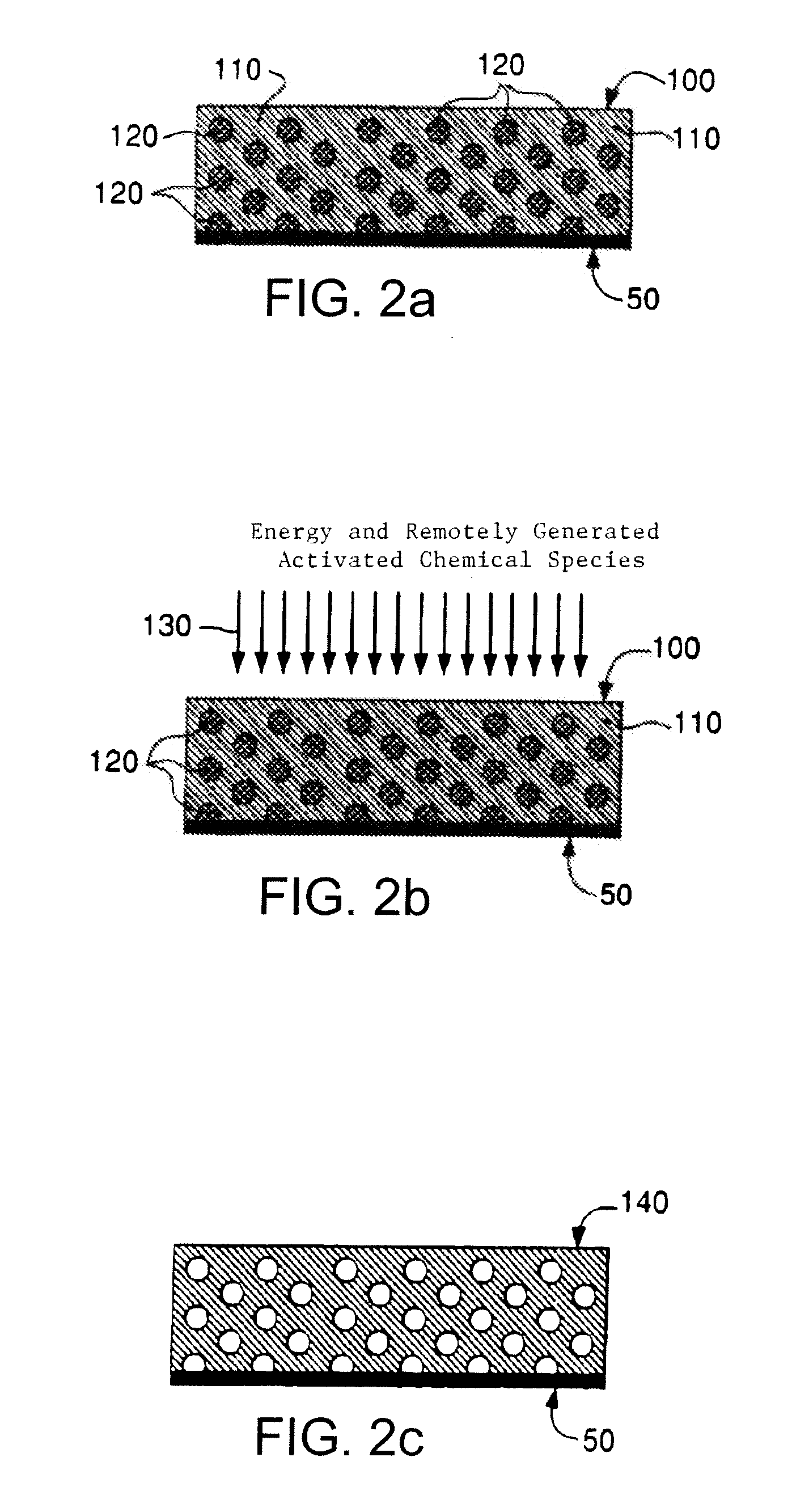
[0100] As illustrated in these examples, the concurrent exposure of composite films to an energy source and a remotely generated activated chemical species effectively and efficiently removes the porogen component of the composite film.

[0101] Composite films are deposited onto a Si substrate using PE-CVD processing techniques as described above, film #1. An activated source of hydrogen is supplied to the UV chamber by a down stream microwave assisted plasma generator with an ion trap to significantly remove the ions from the gas stream. The following conditions are used for the downstream microwave plasma and UV chamber: [0102] Microwave plasma: 1.5 torr; 5000 sccm 5% H2 / He; temperature 350° C.; power 1500 watts [0103] UV source: 6000 watt broad band bulb (Fusion H+), 100% power, vacuum (

[0104] The samples are exposed to the combined activated hydrogen and UV light for 5 minutes with the platen in the UV chamber at 400° C. Upon exposure of the composite film, the porogen ...

Example

Example 3

[0105] Composite films are deposited onto a Si substrate using PE-CVD processing techniques. An activated source of hydrogen is supplied to an e-beam chamber by a down stream microwave assisted plasma generator with an ion trap to significantly remove the ions from the gas stream. The following conditions are used for the downstream microwave plasma and e-beam chamber:

Microwave Plasma:

[0106] 1.5 torr; 5000 sccm 5% H2 / He; temperature 350° C.; power 1500 watts

E-beam Source: [0107] accelerating voltage 4 KeV, amperage 3 mA, 1000 μC dosage, 400° C.

[0108] The samples are exposed to the combined activated hydrogen and e-beam with the platen in the chamber at 400° C. until the dosage reached 1000 μC. Upon exposure of the composite film, the porogen is significantly removed from the film resulting in films with a dielectric constant of 2.5, refractive index of ˜1.3, and an extinction coefficient at 240 nm of 1×10⁻⁴ or less. The use of activated species also increases the rat...


PUM

PropertyMeasurementUnit
Fractionaaaaaaaaaa
Percent by atomaaaaaaaaaa

Abstract

The present invention provides a process for forming a porous dielectric film, the process comprising: forming onto at least a portion of a substrate a composite film comprising Si, C, O, H and Si—CH3 groups, wherein the composite film comprises at least one silicon-containing structure-forming material and at least one carbon-containing pore-forming material; and exposing the composite film to an activated chemical species to at least partially modify the carbon-containing pore-forming material, wherein at least 90% of Si—CH3 species in the as deposited film remains in the film after the exposing step as determined by FTIR.

Description

CROSS-REFERENCE TO RELATED APPLICATIONS [0001] This application claims the benefit of priority under 35 U.S.C. § 119(e) to earlier filed U.S. patent application Ser. No. 60 / 816,896, filed on Jun. 27, 2006, the disclosure of which is incorporated herein by reference in its entirety.BACKGROUND OF THE INVENTION [0002] The present invention relates generally to the formation of porous films. More specifically, the invention relates to porous materials and films comprising same having a low dielectric constant and methods for making same. [0003] There is a continuing desire in the microelectronics industry to increase the circuit density in multilevel integrated circuit devices such as memory and logic chips to improve the operating speed and reduce power consumption. In order to continue to reduce the size of devices on integrated circuits, the requirements for preventing capacitive crosstalk between the different levels of metallization becomes increasingly important. These requirement...

Claims


Application Information

Patent Timeline
IPC IPC(8): C08G69/26
CPCC23C16/401C23C16/56H01L21/02126H01L21/02203H01L21/02216H01L21/31695H01L21/02337H01L21/0234H01L21/02348H01L21/02351H01L21/02274C08J5/18C08J7/12C08J7/18
Inventor WEIGEL, SCOTT JEFFREYO'NEILL, MARK LEONARDVRTIS, RAYMOND NICHOLASHAAS, MARY KATHRYNKARWACKI, EUGENE JOSEPH JR.
Owner VERSUM MATERIALS US LLC
Why Eureka
Try Eureka