Circuit Board And Manufacturing Method Thereof

a technology of circuit board and manufacturing method, which is applied in the direction of high-frequency circuit adaptation, cross-talk/noise/interference reduction, and metal adhesion improvement of insulating substrate, etc., can solve the problems of difficult to deal with high-frequency signals, difficult to transmit noiseless signals in signal transmission in high-frequency range, and possible disconnection. , to achieve the effect of suppressing noise, low surface roughness and high adhesion

Inactive Publication Date: 2008-02-07
OHMI +1
View PDF0 Cites 22 Cited by
  • Summary
  • Abstract
  • Description
  • Claims
  • Application Information

AI Technical Summary

Benefits of technology

[0016]According to this invention, it is possible to provide a circuit board having high adhesion between a conductor layer with a low surface roughness and an electrically insulat

Problems solved by technology

Further, disconnection may also occur due to excessive load applied to a via hole.
However, with the surface roughness of the conductor layer in this circuit board, it has been very difficult to transmit a noiseless signal in signal transmission in a high-frequency range.
Further, with the circuit boar

Method used


Image

  • Circuit Board And Manufacturing Method Thereof
  • Circuit Board And Manufacturing Method Thereof
  • Circuit Board And Manufacturing Method Thereof

Examples


example 1

[0107]8-ethyl-tetracyclo[4.4.0.1 2.5.17.10]-dodeca-3-ene was ring-opening polymerized and then hydrogenated, thereby obtaining a hydrogenated polymer with number average molecular weight (Mn)=31,200, weight average molecular weight (Mw)=55,800, and Tg=approximately 140° C. The hydrogenation ratio of the obtained hydrogenated polymer was 99% or more.

[0108]100 parts of this hydrogenated polymer, 40 parts of maleic anhydride, and 5 parts of dicumyl peroxide were dissolved in 250 parts of t-butylbenzene and the reaction was carried out at 140° C. for 6 hours. An obtained reaction product solution was poured into 1000 parts of isopropyl alcohol to solidify the reaction product and the obtained solid matter was vacuum-dried at 100° C. for 20 hours, thereby obtaining a maleic acid modified hydrogenated polymer. This maleic acid modified hydrogenated polymer had Mn=33,200, Mw=68,300, and Tg=170° C. The maleic anhydride residue content ratio was 25 mol %.

[0109]100 parts of the obtained malei...

example 2

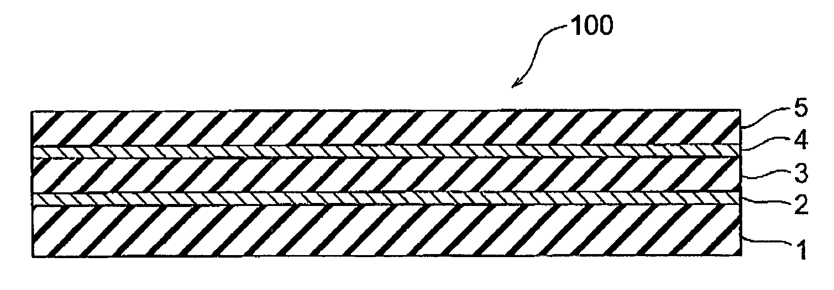
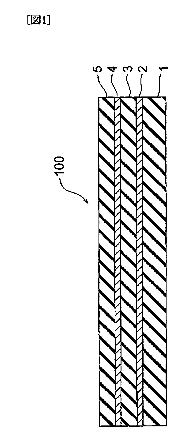
[0120]A wiring pattern-added multilayered circuit board B with four layers on each of both sides was obtained in the same manner as in Example 1 except that the surfaces of the first electrically insulating layers 3 in Example 1 were immersed in the permanganic acid treatment bath for 30 minutes. The surface roughness Ra of the first conductor layers 2 and that of the first electrically insulating layers 3 measured in the processes for obtaining the subject board were 70 nm and 350 nm, respectively. The evaluation results are shown in Table 1 below.

example 3

[0121]100 parts of the foregoing maleic acid modified hydrogenated polymer, 40 parts of bisphenol A bis(propylene glycol glycidyl ether)ether, 0.1 parts of 1-benzyl-2-phenylimidazole (curing accelerator), 5 parts of 2-[2-hydroxy-3,5-bis(α, α-dimethylbenzyl)phenyl]benzotriazole (laser processability improving agent), 1 part of tris(3,5-di-t-butyl-4-hydroxybenzyl)-isocyanurate, 10 parts of liquid polybutadiene (B-1000, Nippon Petrochemicals Company, Ltd.), and 156 parts of a ferrite material (Toda Kogyo Corporation) in the form of fine magnetic substance powder made of an insulator were dissolved in a mixed organic solvent composed of 222 parts of xylene and 555 parts of cyclopentanone, and uniformly dispersed / mixed by the planetary mixer, thereby obtaining a fine magnetic substance powder containing varnish.

[0122]A wiring pattern-added multilayered circuit board C with four layers on each of both sides was obtained in the same manner as in Example 1 except that the fine magnetic subs...


PUM


Abstract

A circuit board having high adhessiveness contact between electrically insulating layers and having a low interlayer electric resistance is provided. A circuit board is provided with a first conductive layer formed on a core (1) and a first electrically insulating layer formed thereon. In the circuit board, a first conductor layer has a surface roughness Ra of 0.1 nm or more but less than 100 nm, and a first primer layer having a thiol compound as a main material is provided between the first conductive layer and the first electrically insulating layer. Thus, the circuit board which has excellent adhesiveness between the first conductor layer and the first electrically insulating layer and is also applicable to high frequency signal is provided.

Description

TECHNICAL FIELD[0001]This invention relates to a circuit board and, more specifically, relates to a circuit board in which adhesion between a conductor layer and an electrically insulating layer or between electrically insulating layers is high and, further, noise of the conductor layer and crosstalk or radiation noise between adjacent conductors (wires) hardly mix with a high-frequency signal flowing in a circuit, an electronic device using the circuit board, and a manufacturing method of the circuit board. Herein, the conductor layer may be either a layer made of only a conductor or a layer including a circuit formed by a conductor.BACKGROUND ART[0002]With electronic devices becoming smaller in size and more multifunctional, higher densification has been required also for circuit boards used in the electronic devices.[0003]As a general technique for densification of a circuit board, it is well known to multilayer the circuit board. The multilayered circuit board is normally obtain...

Claims


Application Information

Patent Timeline
IPC IPC(8): H01B13/00H05K1/02H05K1/03H05K3/38H05K3/46
CPCH05K1/0216H05K1/0242H05K3/389H05K1/024H05K1/05
Inventor OHMI, TADAHIROMORIMOTO, AKIHIROKATO, TAKEYOSHIKAWASAKI, MASAFUMIWAKIZAKA, YASUHIRO
Owner OHMI
Why Eureka
Try Eureka