Nanowires in thin-film silicon solar cells
- Summary
- Abstract
- Description
- Claims
- Application Information
AI Technical Summary
Benefits of technology
Problems solved by technology
Method used
Image

Examples
example 1
[0069]This Example serves to illustrate formation of a conformal layer of amorphous Si on crystalline Si nanowires (formed by an wet etching process), in accordance with some embodiments of the present invention.
[0070]A silicon wafer is bonded to a piece of metal foil or a metallized glass wafer using standard metallurgical bonding methods. The wafer is then thinned to a desired thickness in a standard Si etchant such as a mixture of hydrofluoric, acetic, and nitric acids. Once the desired thickness is reached, typically being 5 μm to 20 μm, the nanowires (representative elongated nanostructures) are formed in the silicon by immersion in a silver nitrate / hydrofluoric acid solution. The conformal i-n junction is formed by plasma-enhanced chemical vapor deposition (PECVD), followed by deposition of a top transparent conducting oxide (TCO). A via is established for backside contact and final top and bottom contacts are formed by a shadow mask deposition process. FIGS. 6 and 7 are scann...
example 2
[0071]This Example serves to illustrate formation of a conformal layer of amorphous Si on CVD-grown crystalline Si nanowires, in accordance with some embodiments of the present invention.
[0072]Silicon nanowires are grown on a conductive substrate material such as stainless steel foil, or a doped ZnO-coated glass wafer, after deposition of a suitable catalyst thin film or nanoparticle layer. In one such embodiment, a nanoporous template layer is first established on top of the back contact material by anodization and then a catalyst is placed within the pores of the template electrochemically. Once the nanowires are grown, the conformal i-n junction is formed by plasma-enhanced chemical vapor deposition (PE-CVD), followed by deposition of a top transparent conducting oxide (TCO). An example of a thick amorphous silicon layer deposited on CVD-grown Si nanowires is shown in FIGS. 8 and 9. FIGS. 8 and 9 are scanning electron microscopy images of conformal amorphous Si layer on a Si nano...
example 3
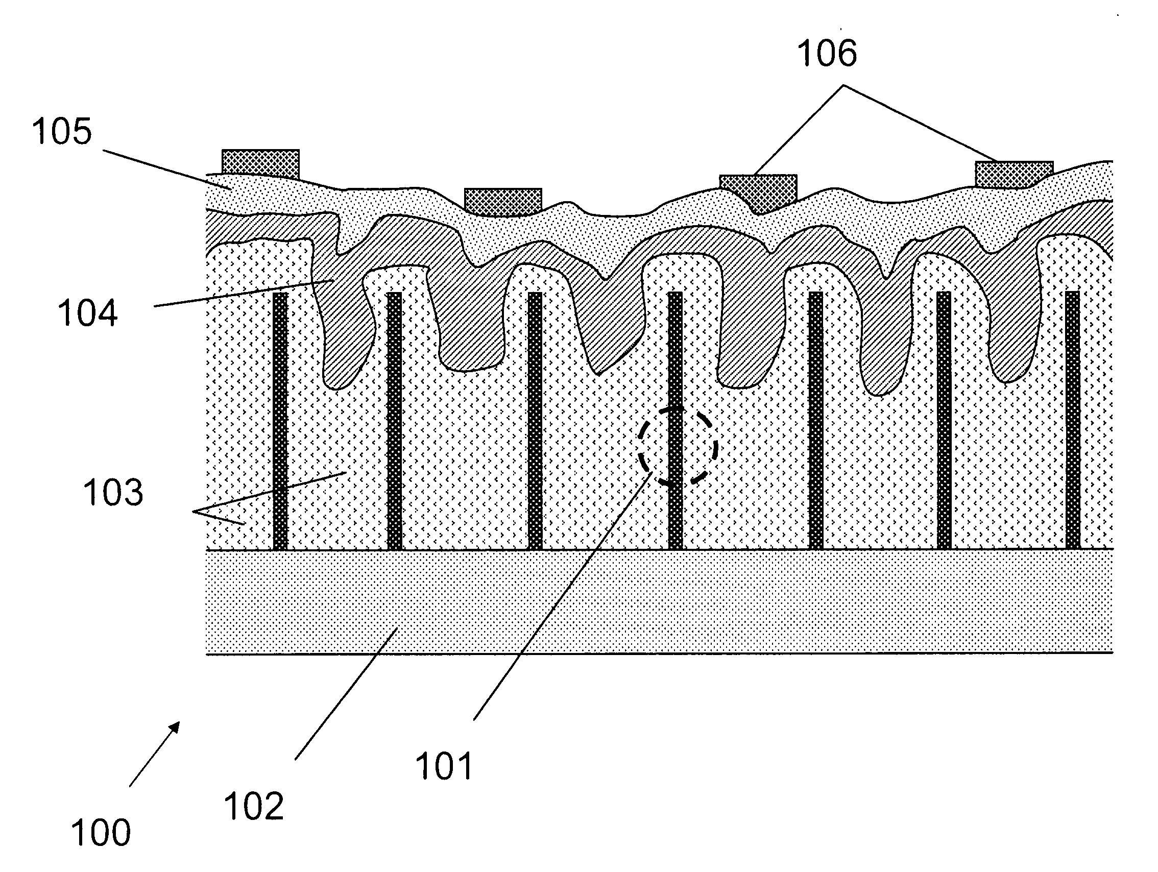
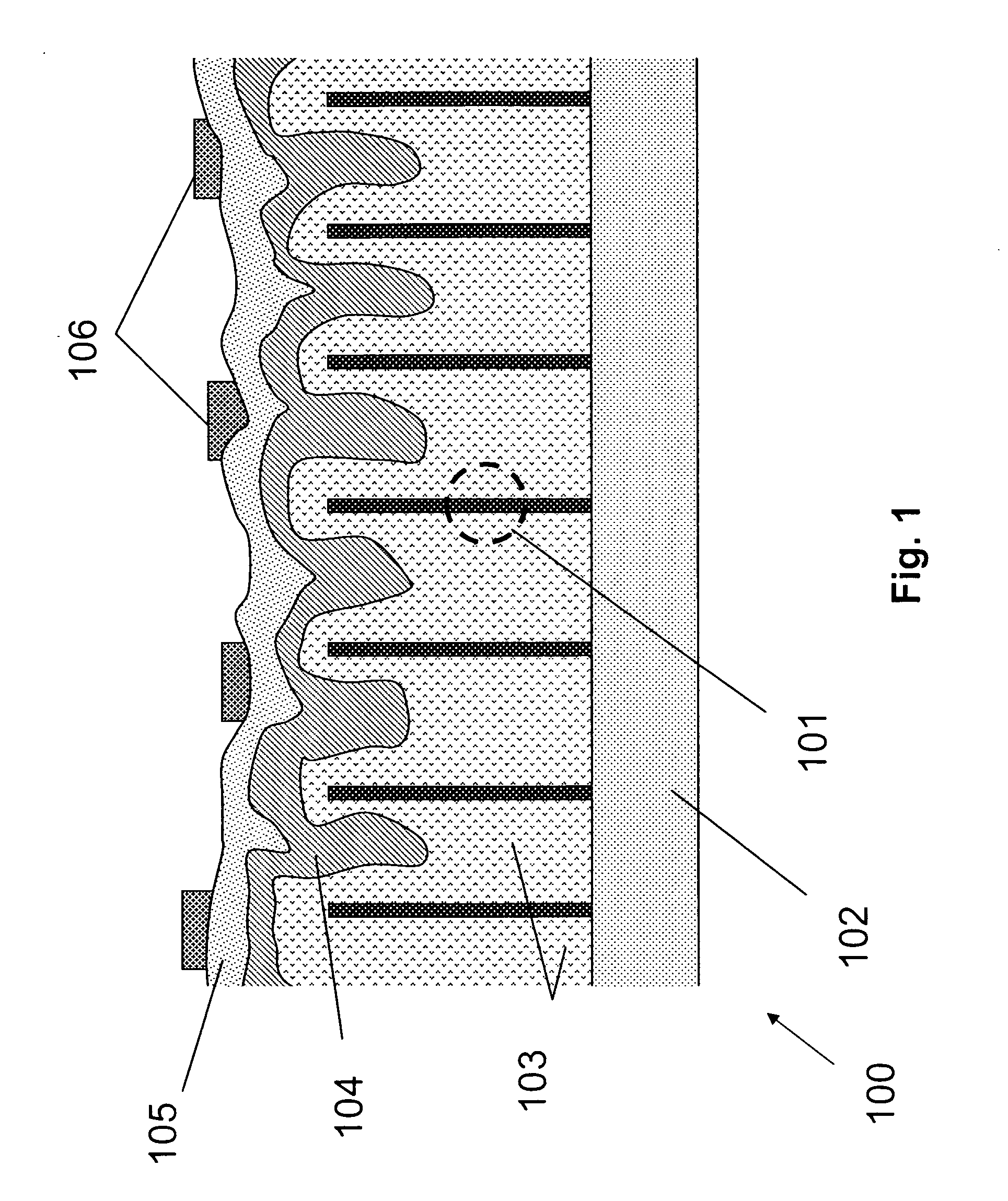
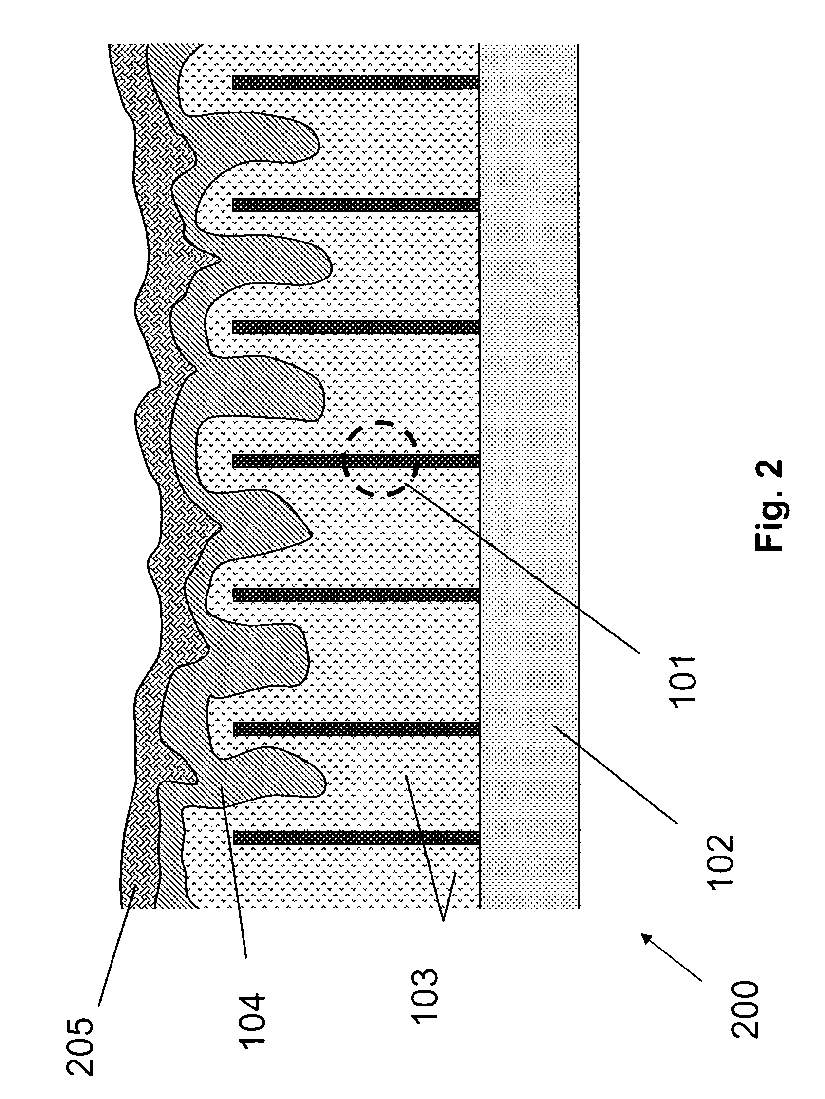
[0073]This Example serves to illustrate an exemplary system comprising photovoltaic devices 100, in accordance with some embodiments of the present invention.
[0074]The photovoltaic device(s) 100 and / or 200 can be packaged in a photovoltaic module such that they are physically isolated from the environment. The module front surface is made of glass to allow sunlight to penetrate, and electrical leads are established on the backside for incorporation into a PV power system. In one embodiment, the photovoltaic device 100 / 200 is grown on a large glass substrate with an intermediate doped ZnO layer such that the glass substrate becomes the protecting glass for the PV module, the original growth layer for the nanowires now being the “front contact” (in terms of the direction in which it is illuminated). Corresponding “backside contact” is then established at the original top surface of the elongated nanostructure layer.
PUM
 Abstract
Description
Claims
Application Information
 - R&D
- Intellectual Property
- Life Sciences
- Materials
- Tech Scout
- Unparalleled Data Quality
- Higher Quality Content
- 60% Fewer Hallucinations
Browse by: Latest US Patents, China's latest patents, Technical Efficacy Thesaurus, Application Domain, Technology Topic, Popular Technical Reports.
© 2025 PatSnap. All rights reserved.Legal|Privacy policy|Modern Slavery Act Transparency Statement|Sitemap|About US| Contact US: help@patsnap.com