Nitride semiconductor laser device and a method for improving its performance
a laser device and nitride technology, applied in the direction of semiconductor lasers, crystal growth process, polycrystalline material growth, etc., can solve the problems of affecting the lifetime of over 100 mw laser diodes, and affecting the performance of nitride semiconductor laser devices. achieve the effect of improving the performance of a nitride semiconductor laser devi
- Summary
- Abstract
- Description
- Claims
- Application Information
AI Technical Summary
Benefits of technology
Problems solved by technology
Method used
Image
Examples
example 1
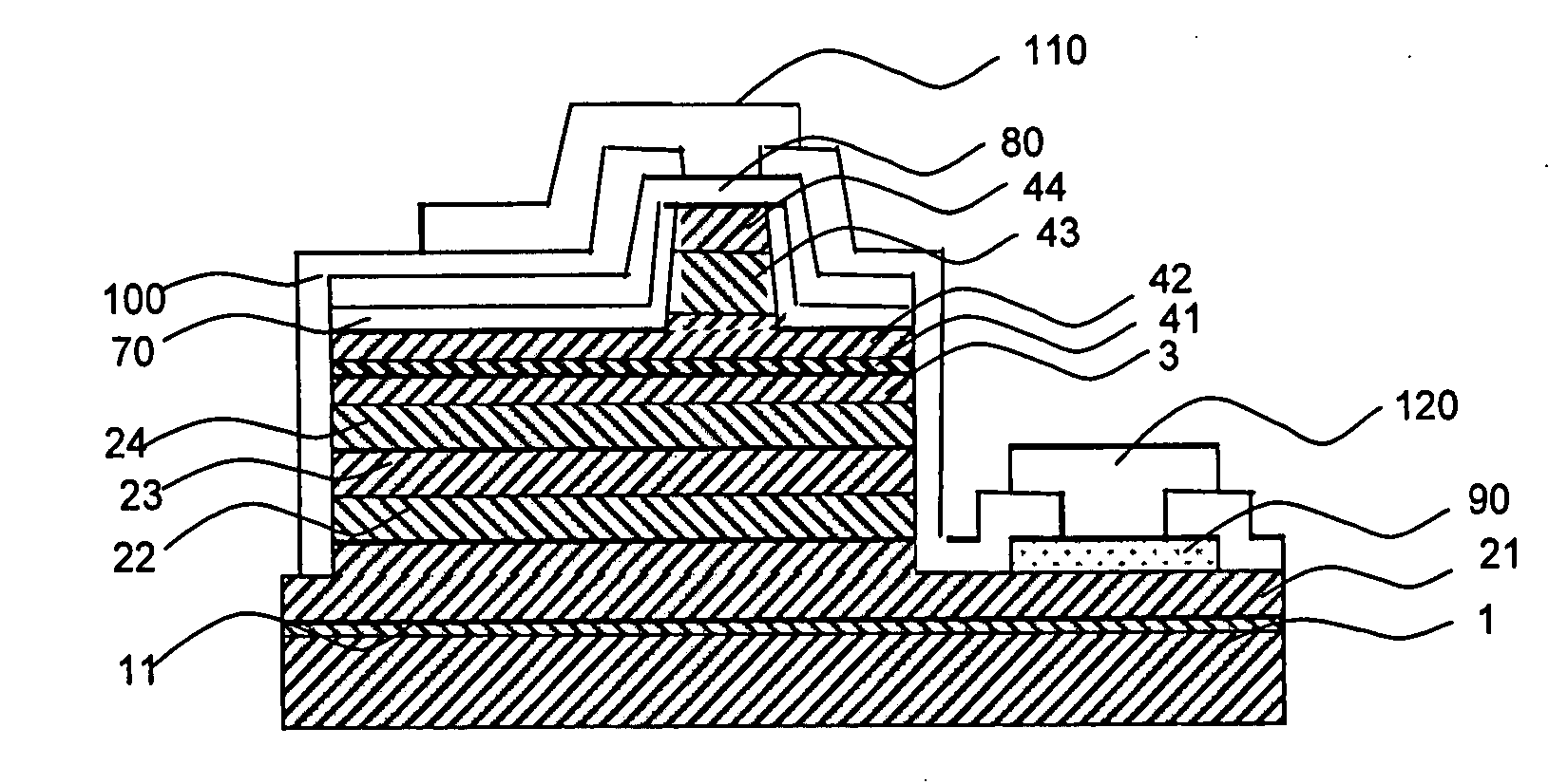
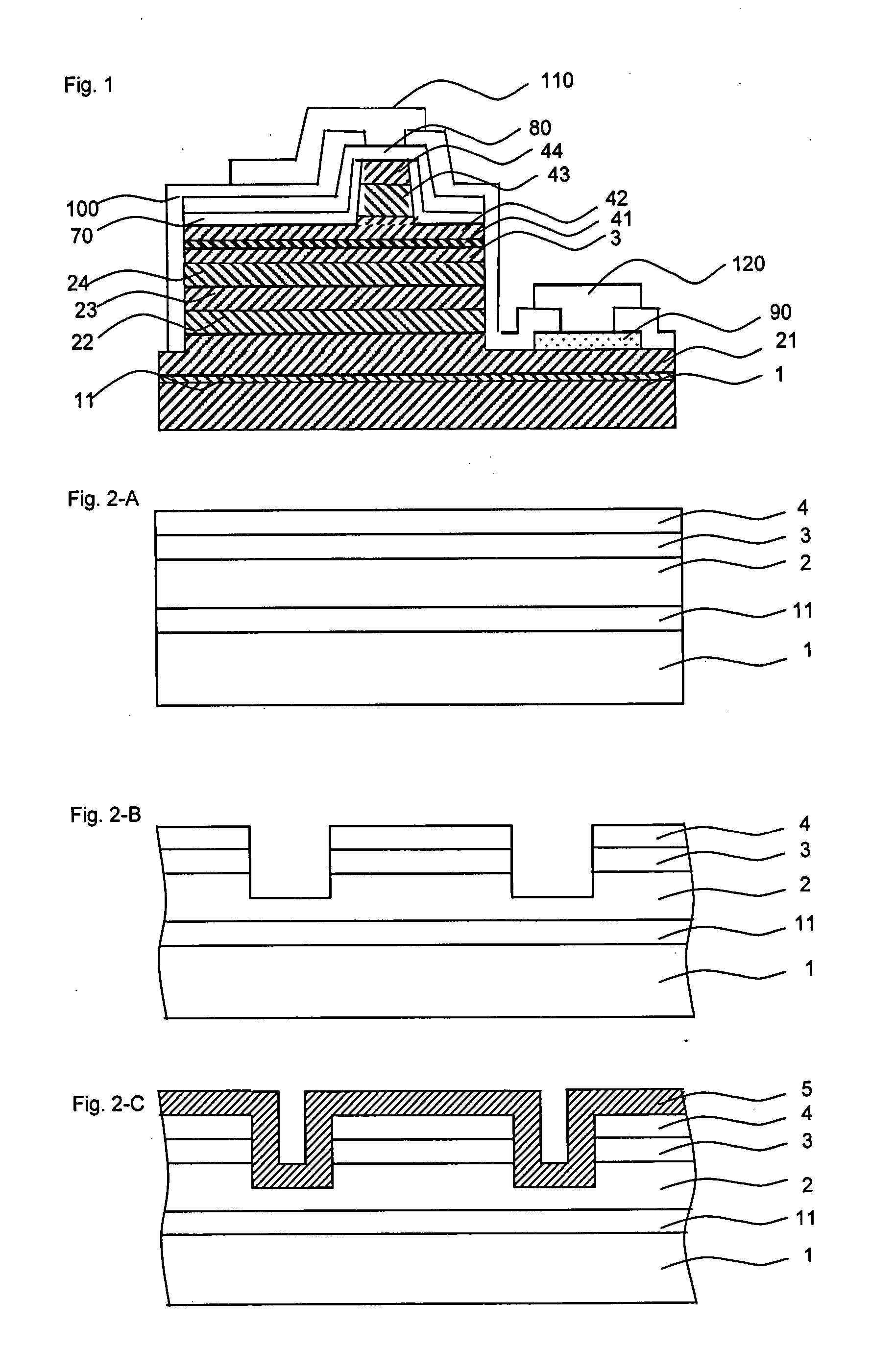
[0111] First, the sapphire wafer 1 of 2 inch diameter and a surface essentially perpendicular to c-axis is placed in the MOCVD reactor. Temperature is set at 510° C. Hydrogen is used as carrier gas and gaseous substrates of the reaction are: ammonia and TMG (thrimethylgallium). The GaN buffer layer 11 of 200 angstrom thick is formed on the sapphire wafer, in the conditions of low-temperature growth.
[0112] On the buffer layer, the following layers are deposited one after the other: [0113] (1) 4 μm thick n-type GaN contact layer, doped with Si at the level of 3×10¹⁸ / cm3. [0114] (2) 1.5 μm thick undoped In0.06Ga0.94N crack-preventing layer. [0115] (3) n-type clad layer, in the form of the superlattice of the total thickness being 1.2 μm, formed by alternate deposition of 25 angstroms thick undoped In0.1Ga0.9N layers and n-type GaN layers doped with Si at the level of 1×10¹⁹ / cm3. [0116] (4) 0.2 μm thick undoped n-type GaN optical guide layer of. [0117] (5) the active layer of the total...
example 2
[0133] In this Example 2, only the resonator radiation-emitting end face is covered with a GaN monocrystalline layer, whereas other stages of laser production are carried out as in Example 1. The laser element made in this way is also equipped with a heat sink. Similar as in Example 1, the average lifetime of the laser—with the threshold current density of 2.0 kA / cm2, the power output of 100 mW and the 405 nm light wavelength—is extended.
example 3
[0134] In this Example 3, after the buffer layer is formed on a sapphire wafer, a 100 μm thick GaN layer is deposited by the HVPE method. Next, as in Example 1, the n-type nitride semiconductor layer, the active layer and the p-type nitride semiconductor layer are formed. Next, sapphire is removed and consequently a homogenous GaN substrate is obtained. In the successive stages, as in Example 1, resonator end faces are uncovered and subsequently covered with a 0.5 μm thick GaN monocrystalline layer crystallized in the environment of a supercritical ammonia-containing solution. In the case of the nitride semiconductor laser thus obtained, its parameters may be expected to get improved as in Example 1.
PUM
| Property | Measurement | Unit |
|---|---|---|
| temperature | aaaaa | aaaaa |
| temperature | aaaaa | aaaaa |
| temperature | aaaaa | aaaaa |
Abstract
Description
Claims
Application Information


